Double diffusion metal-oxide-semiconductor (DMOS) device of integrated driving resistor and method for manufacturing same

A driving resistance and integrated driving technology, which is applied in semiconductor/solid-state device manufacturing, electrical components, semiconductor devices, etc., can solve the problems of input impedance reduction, negative resistance, and fast switching speed, so as to suppress high-frequency oscillation and reduce The effect of switching speed

Inactive Publication Date: 2015-08-26
PEKING UNIV FOUNDER GRP CO LTD +1
View PDF4 Cites 10 Cited by
  • Summary
  • Abstract
  • Description
  • Claims
  • Application Information

AI Technical Summary

Problems solved by technology

[0003] refer to figure 1 , DMOS devices are composed of hundreds of DMOS units with a single structure. The number of these units is determined according to the driving capability required by a chip. The performance of DMOS devices directly determines the driving capability and chip area of ​​the chip. , so the performance of the DMOS unit is also very important, but when the DMOS unit is in a high-frequency state, due to the decrease of the input impedance, it even becomes a negative resistance in a certain frequency range, resulting in too fast switching speed, which causes high-frequency oscillation

Method used


Image

  • Double diffusion metal-oxide-semiconductor (DMOS) device of integrated driving resistor and method for manufacturing same
  • Double diffusion metal-oxide-semiconductor (DMOS) device of integrated driving resistor and method for manufacturing same
  • Double diffusion metal-oxide-semiconductor (DMOS) device of integrated driving resistor and method for manufacturing same

Examples


Embodiment

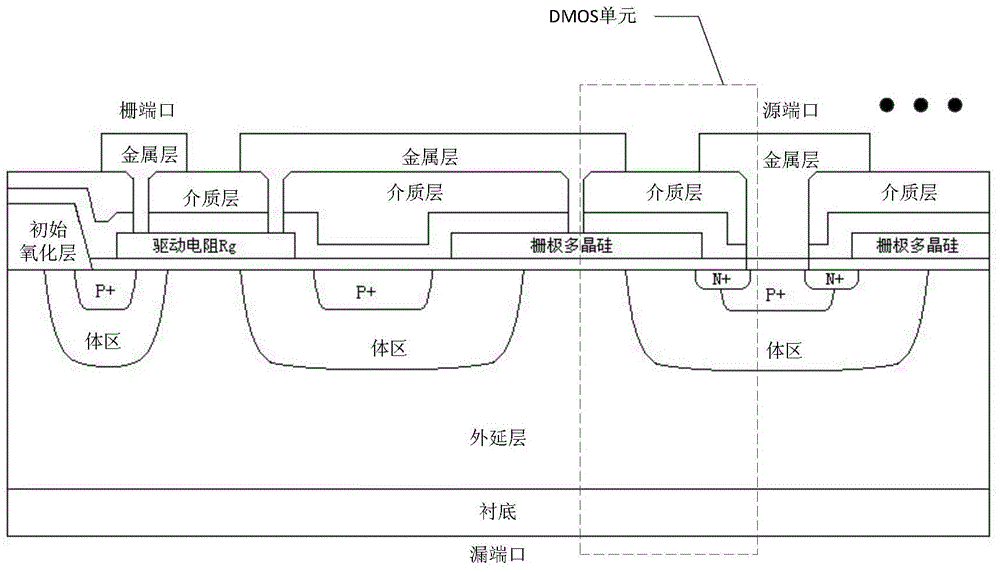
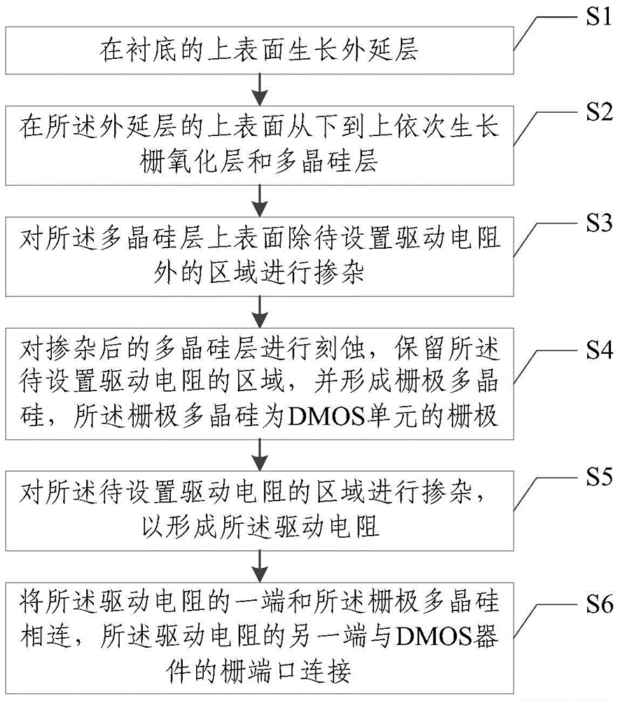
[0085] The manufacturing method of the present invention is described below with a specific embodiment, but the protection scope of the present invention is not limited. The manufacturing method of this embodiment includes the following steps:

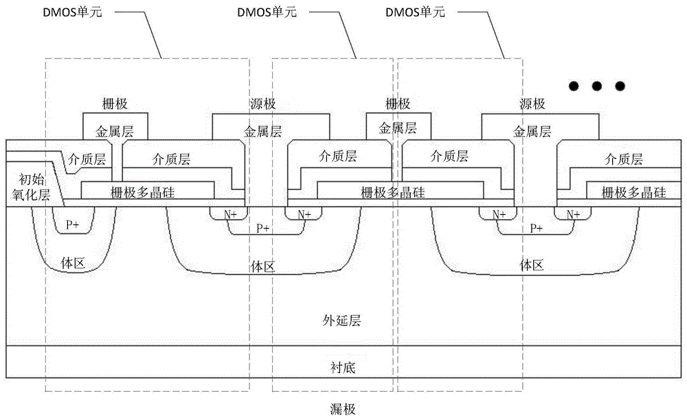
[0086] 1. Reference Figure 4 , grow an epitaxial layer (that is, "N-EPI" in the figure) on the upper surface of the substrate (that is, "N+Sub" in the figure), and grow an initial oxide layer on the upper surface of the epitaxial layer (that is, "N+Sub" in the figure) Int-OX");

[0087] 2. Reference Figure 5 , strip off the initial oxide layer, and open the active area (the initial oxide layer needs to be left at the position of the terminal structure, for the convenience of description, the terminal structure is omitted here and in subsequent steps);

[0088] 3. Reference Figure 6 , growing a gate oxide layer and a polysilicon layer sequentially from bottom to top in the upper surface active region of the epitaxial layer;

[0...


PUM


Abstract

The present invention discloses a DMOS device of an integrated driving resistor and a method for manufacturing the same, and relates to the semiconductor technology field. The DMOS device comprises a grid port, a driving resistor and a plurality of DMOS units. Each DMOS unit comprises a grid, the grid port is connected with one end of the driving resistor, and the other end of the driving resistor is connected with the grid of each DMOS unit separately. According to the present invention, by arranging the driving resistor of the grid port in the DMOS device, the on-off speeds of the DMOS units are reduced, and the high frequency oscillation is restrained.

Description

technical field [0001] The invention relates to the technical field of semiconductors, in particular to a DMOS device integrating a driving resistor and a manufacturing method thereof. Background technique [0002] The DMOS device is similar to the Complementary Metal Oxide Semiconductor (CMOS) structure, and also has electrodes such as source, drain, and gate, but the breakdown voltage of the drain terminal is high. There are two main types of DMOS devices, VDMOSFET (vertical double-diffused MOSFET) and LDMOSFET (lateral double-dif fused MOSFET). [0003] refer to figure 1 , DMOS devices are composed of hundreds of DMOS units with a single structure. The number of these units is determined according to the driving capability required by a chip. The performance of DMOS devices directly determines the driving capability and chip area of ​​the chip. , so the performance of the DMOS unit is also crucial, but when the DMOS unit is in a high-frequency state, due to the decrease...

Claims


Application Information

Patent Timeline
Patent Type & Authority Applications(China)
IPC IPC(8): H01L29/78H01L21/336
CPCH01L29/66712H01L29/7803
Inventor 蔡远飞何昌姜春亮
Owner PEKING UNIV FOUNDER GRP CO LTD
Why Eureka
Try Eureka