

Defect observation method and defect observation device
A technology for observing devices and defects, applied in measuring devices, image data processing, instruments, etc., can solve problems such as failure of defect detection, inability to recognize periodic patterns, inability to synthesize reference images, etc., and achieve the effect of high-precision defect detection
- Summary
- Abstract
- Description
- Claims
- Application Information
AI Technical Summary
Problems solved by technology
Method used
Image

Examples
Embodiment 1
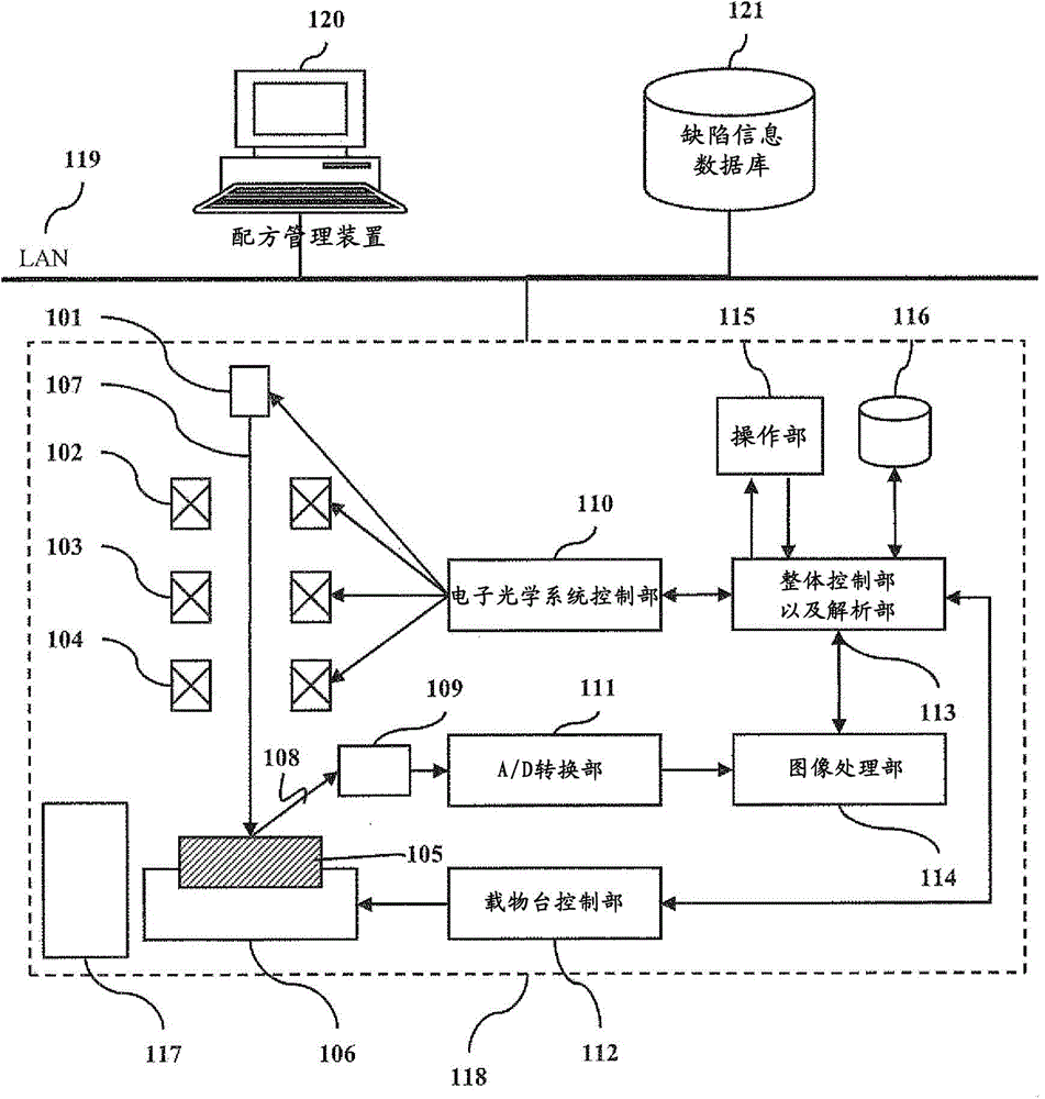
[0046] The SEM defect observation device is a device that takes defect coordinates detected by defect inspection devices such as optical or SEM inspection devices as input information, and obtains high-quality SEM images of defect coordinates under conditions suitable for observation or analysis. As input information to the SEM observation device, coordinate information of observation points extracted by simulation based on design layout data may be used in addition to defect coordinates detected by the defect inspection device.
[0047] figure 1 It is a schematic diagram showing the overall structure of the SEM observation system of this example. figure 1The SEM-type defect observation device 118 is composed of the following components: an electron optical system composed of optical elements such as an electron gun 101, a lens 102, a scanning deflector 103, an objective lens 104, a sample 105, and a secondary particle detector 109; The stage 106 that moves the sample stage o...
Embodiment 2
[0078] In this embodiment, an example of a defect observation method in which the stability of defect detection is more important than the processing speed will be described as compared with the method described in Embodiment 1. Figure 1 to Figure 3 structure and Figure 4 to Figure 7 The content of the description is the same as that of this embodiment, so the description is omitted.
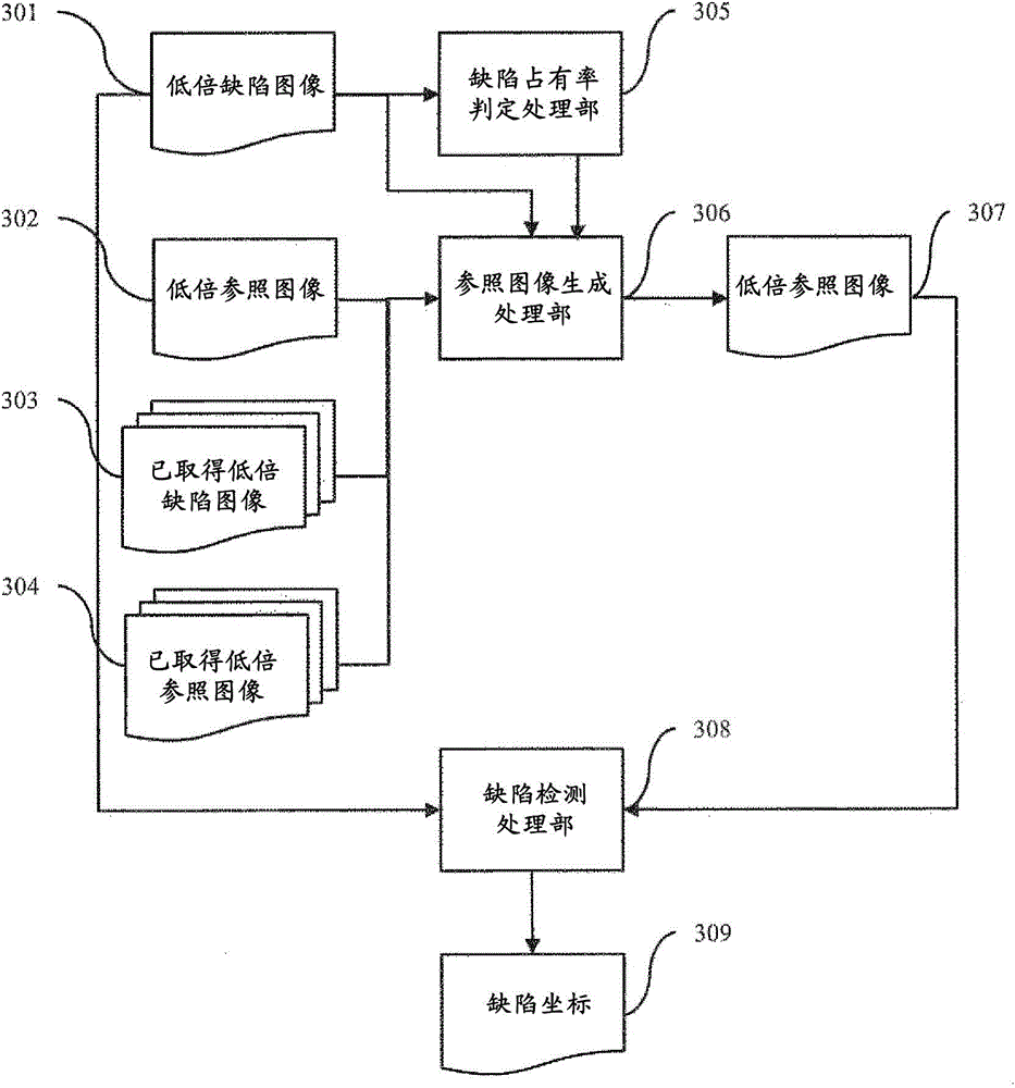
[0079] Figure 8 is expressed in Image 6 and Figure 7 Schematic diagram illustrating the problem of the defect detection method using the low-magnification reference image generated from the average brightness value of the low-magnification defect image. The problem when generating a low-magnification reference image based on the average brightness value of a low-magnification defective image is that the calculated average brightness value is affected by the brightness value of the defective region when the defective area occupies a relatively large area in the low-magnification defective...
Embodiment 3
[0090] In this example, an example of a defect observation method that places emphasis on the stability of defect detection and minimizes a decrease in processing speed compared to the method described in Example 1 will be described. In addition, compared with Example 2, the stability of defect detection was the same, and the processing speed was high. in addition, Figure 1 to Figure 3 structure and Figure 4 to Figure 7 The content of the description is the same as that of this embodiment, so the description is omitted.
[0091] The method described in Example 2 is the same as in Figure 5 Similar to the method of obtaining representative reference images described in , there is a problem that it is easily affected by the noise of low-magnification reference images, and the accuracy of defect detection decreases. In addition, it can be controlled by adjusting the magnification when the low-magnification defect image is acquired, but if Figure 9 As mentioned above, when ...
PUM
 Abstract
Description
Claims
Application Information