Semiconductor structure possessing vertical through hole interconnection and manufacturing method thereof
A vertical via hole and semiconductor technology, which is applied in semiconductor/solid-state device manufacturing, semiconductor devices, semiconductor/solid-state device components, etc., can solve problems such as thermal expansion coefficient mismatch, difficult thermodynamic reliability problems, and thermodynamic reliability threats. Achieve the effect of improving thermal stress problem and improving thermodynamic reliability
- Summary
- Abstract
- Description
- Claims
- Application Information
AI Technical Summary
Problems solved by technology
Method used
Image

Examples
Embodiment 1
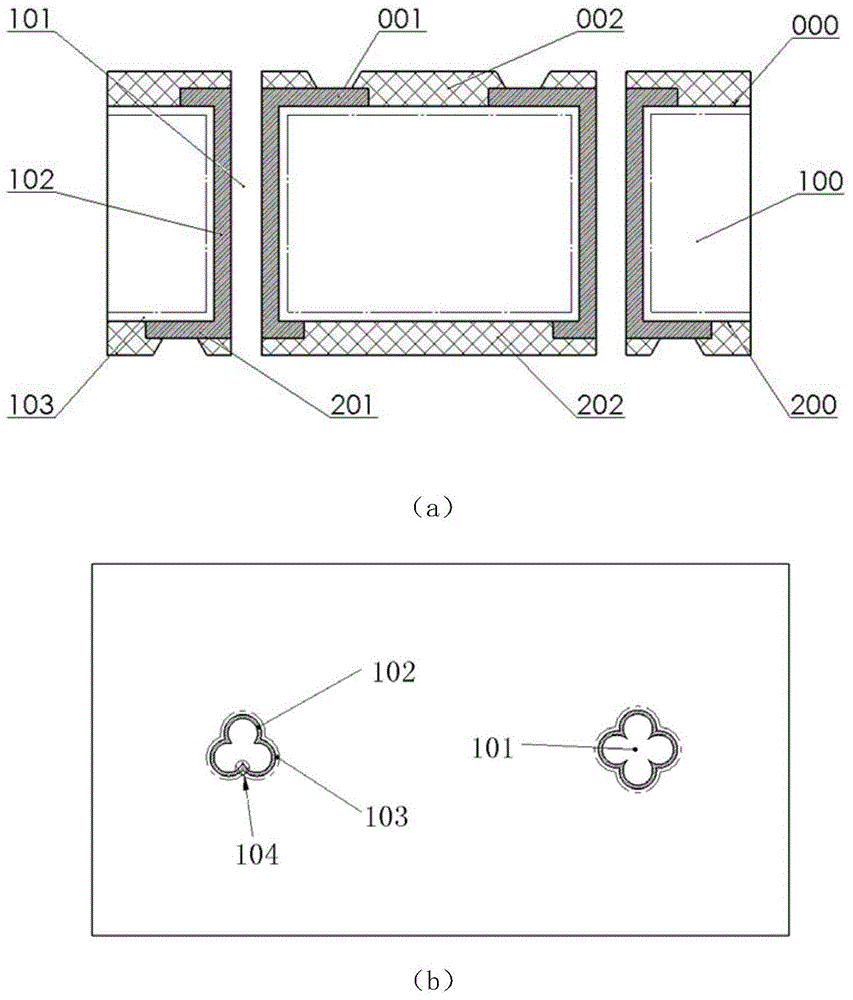
[0031] The semiconductor structure with through-silicon vias disclosed in this embodiment can refer to figure 1 , the semiconductor structure includes a substrate 100, a plurality of petal-shaped vertical via interconnections and a metal interconnection layer, wherein:
[0032] The substrate 100 is silicon or glass, having opposite first surface 000 and second surface 200;
[0033] The petal-shaped vertical through-hole interconnection consists of a vertical through-hole 101 embedded in the substrate with a petal-shaped cross-section vertically penetrating through the first surface 000 and the second surface 200 of the substrate, and A metal layer 102 conformally covering the sidewall of the vertical via hole;
[0034] There are metal interconnection layers on the first surface 000 and the second surface 200 of the substrate respectively, and the metal interconnection layers are respectively composed of conductive metal layers 001, 201 and dielectric layers 002, 202;
[0035...
Embodiment 2
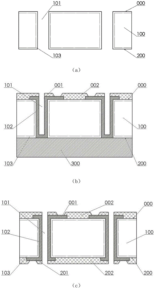
[0039] This embodiment discloses a semiconductor structure manufacturing method with vertical via interconnection, which can be referred to figure 2 , combined below figure 2 To further describe the method:
[0040] Step 1, providing a substrate 100, the substrate is a silicon wafer or a glass wafer, the substrate 100 has an opposite first surface 000 and a second surface 200, and a plurality of flower petal cross-sections are fabricated in the substrate. Shaped shaped through hole 101, such as figure 2 As shown in (a); the cross-section of the special-shaped through hole 101 can be three or four petals, and has a convex free end. The special-shaped through hole 101 is made by deep reactive ion etching (DRIE), laser ablation, sandblasting, Ultrasonic processing, etc.;
[0041] If the substrate used is a silicon wafer, after making the special-shaped through hole 101, it also includes forming an insulating layer 103 on the side wall of the through hole. The insulating lay...
Embodiment 3
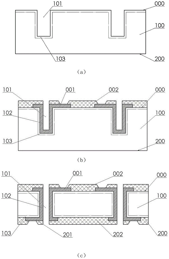
[0045] This embodiment discloses a semiconductor structure manufacturing method with vertical via interconnection, which can be referred to image 3 , which will be combined below image 3 To further explain this method:
[0046] In step 1, the substrate 100 has opposite first surface 000 and second surface 200, and a plurality of petal-shaped shaped blind holes 101 are fabricated in the substrate, such as image 3 As shown in (a); the cross-section of the special-shaped blind hole 101 can be three or four petals, with a convex free end, and the special-shaped through hole 101 is made by deep reactive ion etching (DRIE), laser ablation, sandblasting, Ultrasonic processing, etc.;
[0047] If the substrate used is a silicon wafer, after making the special-shaped through hole 101, it also includes forming an insulating layer 103 on the side wall of the through hole. The insulating layer 103 can have a one-layer or multi-layer structure, and its material is oxide Silicon, silic...
PUM
 Abstract
Description
Claims
Application Information
 - R&D
- Intellectual Property
- Life Sciences
- Materials
- Tech Scout
- Unparalleled Data Quality
- Higher Quality Content
- 60% Fewer Hallucinations
Browse by: Latest US Patents, China's latest patents, Technical Efficacy Thesaurus, Application Domain, Technology Topic, Popular Technical Reports.
© 2025 PatSnap. All rights reserved.Legal|Privacy policy|Modern Slavery Act Transparency Statement|Sitemap|About US| Contact US: help@patsnap.com