Negative voltage level converting circuit inhibiting DC path

A DC path and conversion circuit technology, applied in the direction of logic circuit connection/interface layout, etc., can solve the problem of uncertainty of the working state of the level conversion circuit, and achieve the effect of ensuring high-reliability conversion, ensuring normal operation, and suppressing DC leakage.

Inactive Publication Date: 2015-09-02
NO 771 INST OF NO 9 RES INST CHINA AEROSPACE SCI & TECH
View PDF5 Cites 5 Cited by
  • Summary
  • Abstract
  • Description
  • Claims
  • Application Information

AI Technical Summary

Problems solved by technology

[0011] The purpose of the present invention is to provide a negative voltage level conversion circuit for suppressing the DC path in view of the defects in the above-mentioned prior art, so as to solve the forward-conducting phenomenon of the PN junction of the transistor caused by the uncertainty of the pre-stage Vneg, and avoid the gap between the power supply and Vneg. The DC leakage path, and the uncertainty of the working status of each node of the level conversion circuit caused by the uncertainty of Vneg, so as to ensure that the circuit level conversion circuit can work normally under any conditions

Method used


Image

  • Negative voltage level converting circuit inhibiting DC path
  • Negative voltage level converting circuit inhibiting DC path

Examples


Embodiment Construction

[0023] The present invention will be described in further detail below in conjunction with the accompanying drawings.

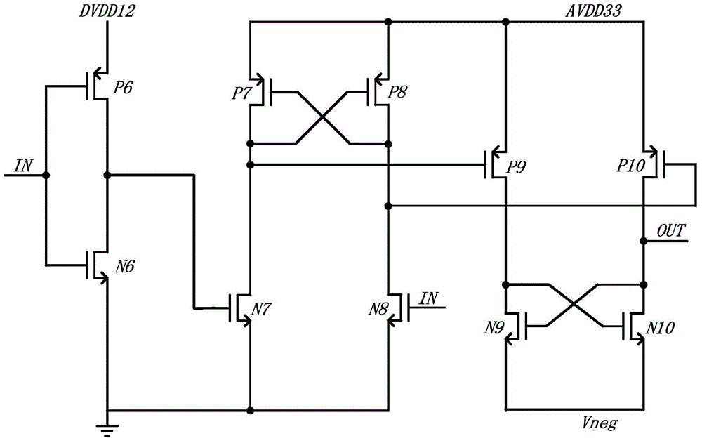
[0024] see figure 2 , the negative voltage level conversion circuit of the present invention includes five P-channel metal oxide semiconductor field effect transistors P6, P7, P8, P9, P10, and five N-channel metal oxide semiconductor field effect transistors N6, N7, N8 , N9, N10.

[0025] For the convenience of description, the P-channel MOSFET and the N-channel MOSFET will be referred to as P tube and N tube below.

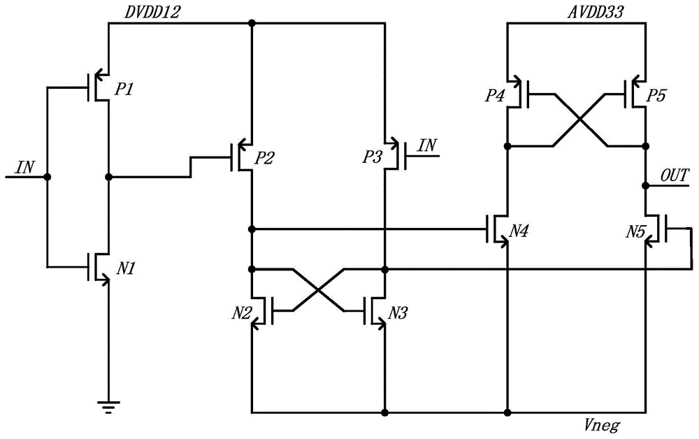
[0026] DVDD12 is the 1.2V power supply voltage of the digital circuit, AVDD33 is the 3.3V power supply voltage of the analog circuit, and Vneg is a negative voltage signal. IN is an input signal between 0 and DVDD12, and OUT is an output signal between Vneg and AVDD33.

[0027] The negative voltage level conversion circuit of the present invention shown in the figure mainly includes the following branches:

[0028] The first branch, this br...


PUM


Abstract

A negative voltage level converting circuit inhibiting a DC path comprises five P channel metal-oxide semiconductor field effect transistors P6, P7, P8, P9 and P10, and five N channel metal-oxide semiconductor field effect transistors N6, N7, N8, N9 and N10; the circuit converts a 0V-digit circuit power supply voltage into 0V-simulation circuit power supply voltage, then converts the 0V-simulation circuit power supply voltage into negative voltage power supply voltage Vneg-simulation circuit power supply voltage, thus solving uncertainty problems of each node work state of the level converting circuit because of uncertainty of the Vneg; the negative voltage level converting circuit can inhibit the digit circuit power supply-negative voltage power supply DC path caused by PN junction positive conduction when the Vneg is uncertain, thus ensuring normal working of the level converting circuit.

Description

technical field [0001] The invention belongs to the field of integrated circuit design, and in particular relates to a negative voltage level conversion circuit for suppressing a direct current path. Background technique [0002] During the operation of an integrated circuit, different voltages are generally required for different application scenarios. For example, in a high-speed chip interface circuit, different levels cannot be directly interconnected, and corresponding level conversion circuits are required for connection. Therefore, the level conversion circuit that converts the input voltage to the corresponding voltage in different scenarios has become a direction that integrated circuit designers must overcome. [0003] figure 1 Shown is a typical negative voltage level conversion circuit structure in the existing common technology in the industry. IN is the input signal between 0 and DVDD12, OUT is the output signal between Vneg and AVDD33, where DVDD12 is the 1...

Claims


Application Information

Patent Timeline
Patent Type & Authority Applications(China)
IPC IPC(8): H03K19/0175
Inventor 肖筱
Owner NO 771 INST OF NO 9 RES INST CHINA AEROSPACE SCI & TECH
Why Eureka
Try Eureka