Semiconductor device and manufacturing method thereof

A manufacturing method and semiconductor technology, applied in the direction of semiconductor/solid-state device manufacturing, semiconductor devices, electrical components, etc., can solve the problems of limited current conduction cross-sectional area, limitation, and increased component size, so as to improve the driving current and reduce the On-resistance, the effect of increasing the conduction cross-sectional area

Active Publication Date: 2018-10-26
VANGUARD INTERNATIONAL SEMICONDUCTOR CORPORATION
View PDF5 Cites 0 Cited by
  • Summary
  • Abstract
  • Description
  • Claims
  • Application Information

AI Technical Summary

Problems solved by technology

However, the pillar-type N-type doped region and pillar-type P-type doped region of this technology are limited by the depth that can be reached by ion implantation and subsequent thermal diffusion, so the cross-sectional area of ​​current conduction is also limited
To increase the total surface area of ​​the N-type doped region and the P-type doped region, the size of the element must be increased

Method used


Image

  • Semiconductor device and manufacturing method thereof
  • Semiconductor device and manufacturing method thereof
  • Semiconductor device and manufacturing method thereof

Examples


Embodiment Construction

[0042] Embodiments for practicing the invention are discussed in detail below. It will be appreciated that the embodiments provide many applicable inventive concepts, which can be implemented in wide variation. The specific embodiments discussed are merely illustrative of specific ways to use the embodiments and do not limit the scope of the invention. In order to make the features of the present invention more comprehensible, the specific examples below are described in detail in conjunction with the accompanying drawings:

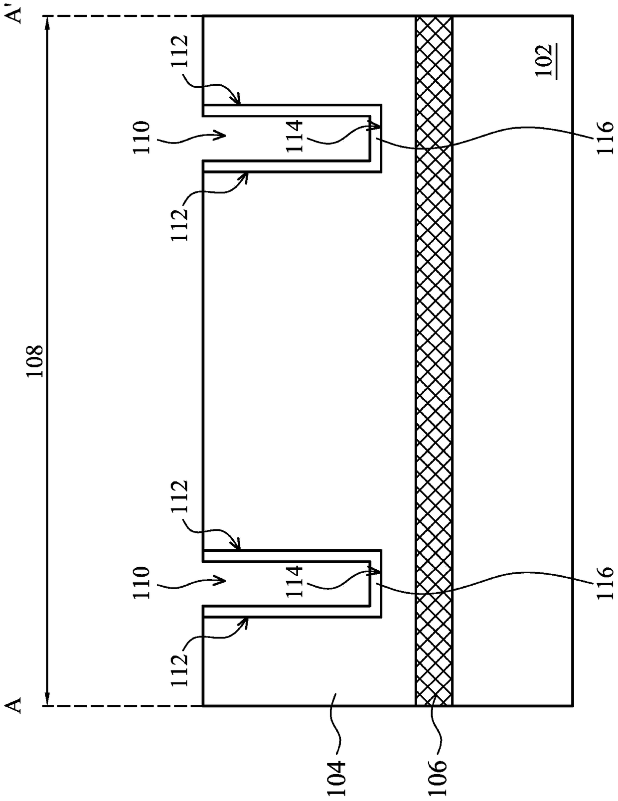
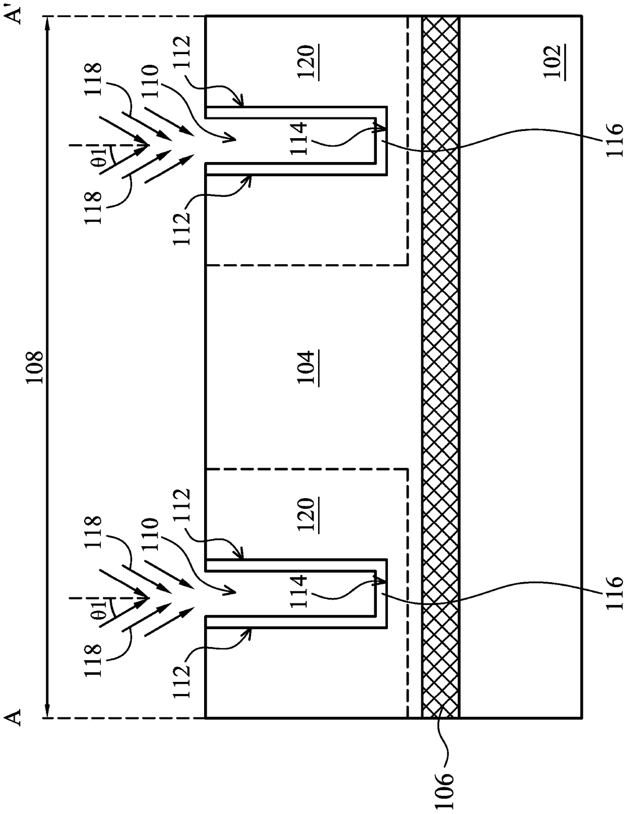
[0043] image 3 A perspective view showing a semiconductor device with a super junction structure according to an embodiment of the present invention. Figure 1A-1E showing an embodiment of the invention along image 3 A-A' cross-sectional view of intermediate fabrication steps of a semiconductor device.

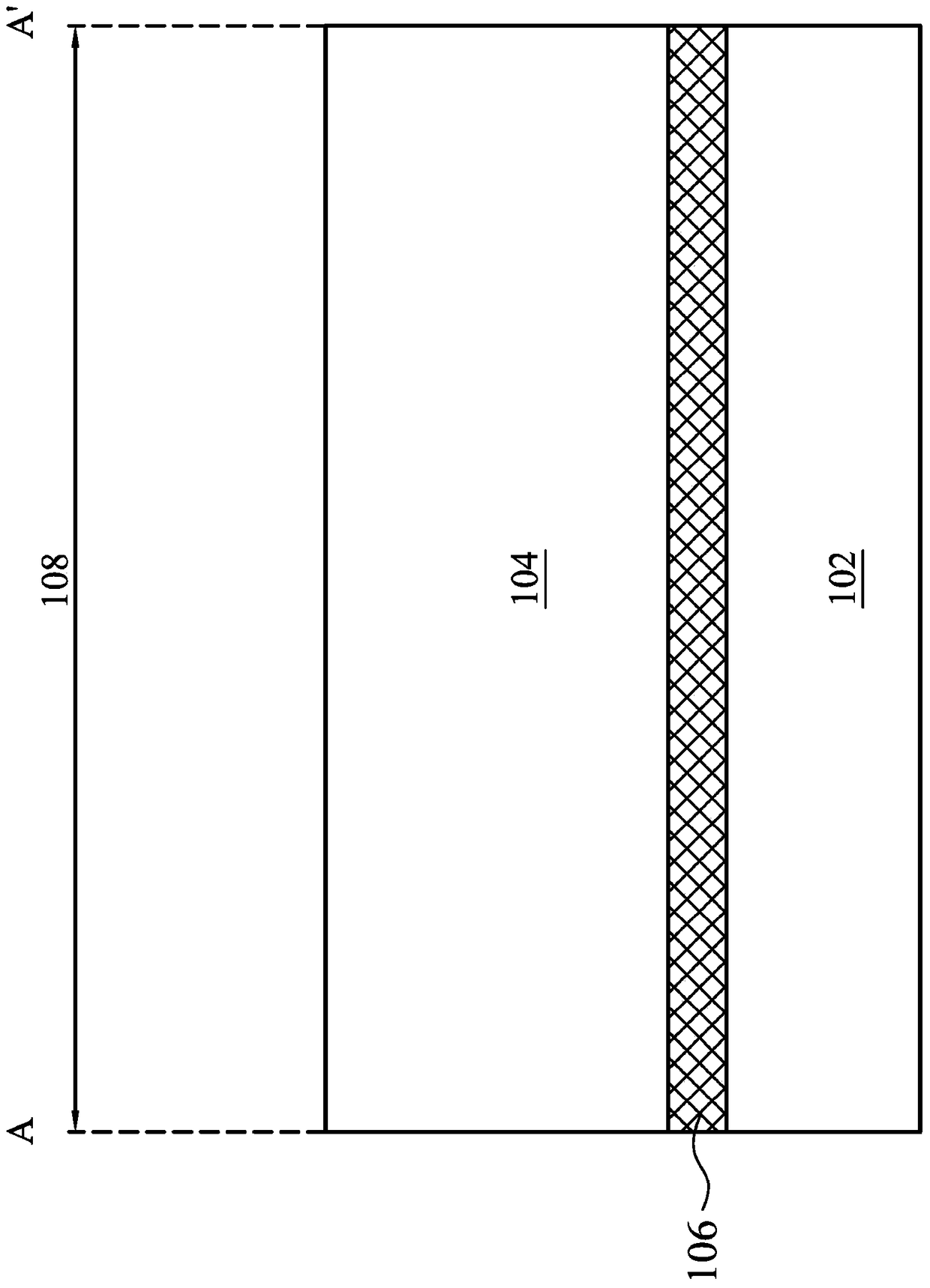
[0044] Please refer to Figure 1A , providing a semiconductor substrate 102 having a first conductivity type. Thereafter, an insulating layer 106...


PUM


Abstract

A semiconductor device and its manufacturing method, the semiconductor device includes: a substrate; and an epitaxial layer located above the substrate, wherein the epitaxial layer includes a plurality of first grooves and a plurality of second trenches arranged alternately along a first direction Groove; wherein the epitaxial layer between each adjacent first groove and second groove includes a first doped region and a second doped region, and the first doped region and the second doped region have different The conductivity type, and the interface between the first doped region and the second doped region forms a super junction structure; and a gate structure, located above the epitaxial layer, wherein the epitaxial layer below the gate structure includes along a second A channel extending in a direction, wherein the first direction is perpendicular to the second direction. Compared with the prior art, the present invention can increase the conduction cross-sectional area of ​​the drive current, improve the drive current and reduce the conduction resistance.

Description

technical field [0001] The present invention relates to a semiconductor technology, in particular to a semiconductor device with a super junction structure and a manufacturing method thereof. Background technique [0002] The existing vertical diffused metal oxide semiconductor field effect transistor (VDMOSFET) mainly forms a P-N junction by an N-type epitaxy (Epitaxy) drift region (Drift region) and a P-type base (Base) doping region above it, and the semiconductor element The withstand voltage is mainly borne by the P-N junction. When increasing the operating voltage of a semiconductor device, it is necessary to reduce the dopant concentration and increase the thickness of the N-type epitaxial drift region. In contrast, the above method of increasing the withstand voltage of the P-N junction will also increase the on-resistance (Ron) of the device, and the on-resistance is also limited by the dopant concentration and thickness of the N-type epitaxial drift region. The d...

Claims


Application Information

Patent Timeline
Patent Type & Authority Patents(China)
IPC IPC(8): H01L29/78H01L29/06H01L21/336
CPCH01L29/0603H01L29/66477H01L29/78H01L29/7824H01L29/0634H01L29/66681
Inventor 李琮雄张睿钧张雄世
Owner VANGUARD INTERNATIONAL SEMICONDUCTOR CORPORATION
Why Eureka
Try Eureka