Power supply device and manufacturing method of printed circuit board winding

A technology for printed circuit boards and power supply devices, applied in the directions of printed circuits, printed circuits, printed circuit components, etc., can solve the problems of reducing the on-resistance of conductive windings, increasing the conductive layer inside the PCB, and unable to solve the on-resistance, etc. The effect of increasing the conduction cross-sectional area, improving the heat dissipation efficiency and reducing the skin effect

Active Publication Date: 2013-08-28
HUAWEI TECH CO LTD
View PDF4 Cites 0 Cited by
  • Summary
  • Abstract
  • Description
  • Claims
  • Application Information

AI Technical Summary

Problems solved by technology

Therefore, the on-resistance problem cannot be solved simply by increasing the thickness of the conductive layer inside the PCB.
Moreover, under the demand of high power density modules, the volume occupied by each module is gradually reduced, and the plane area occupied by the conductive layer is also gradually reduced. In this case, reducing the conduction resistance of the conductive winding on the power supply PCB becomes technical challenge

Method used


Image

  • Power supply device and manufacturing method of printed circuit board winding
  • Power supply device and manufacturing method of printed circuit board winding
  • Power supply device and manufacturing method of printed circuit board winding

Examples


Embodiment 1

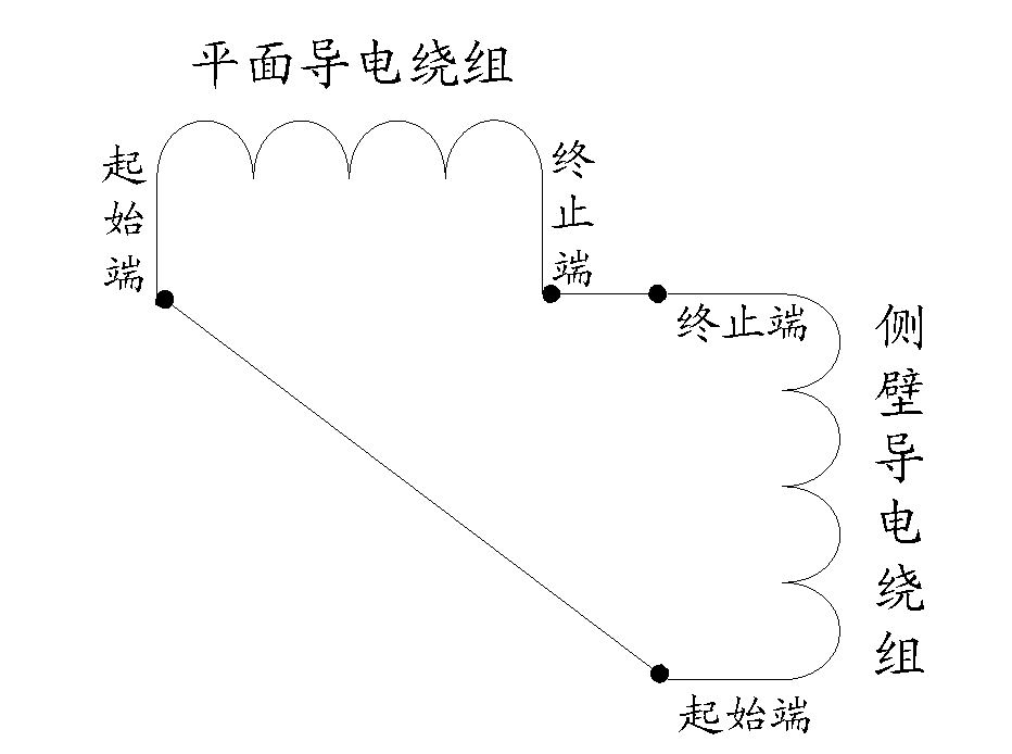
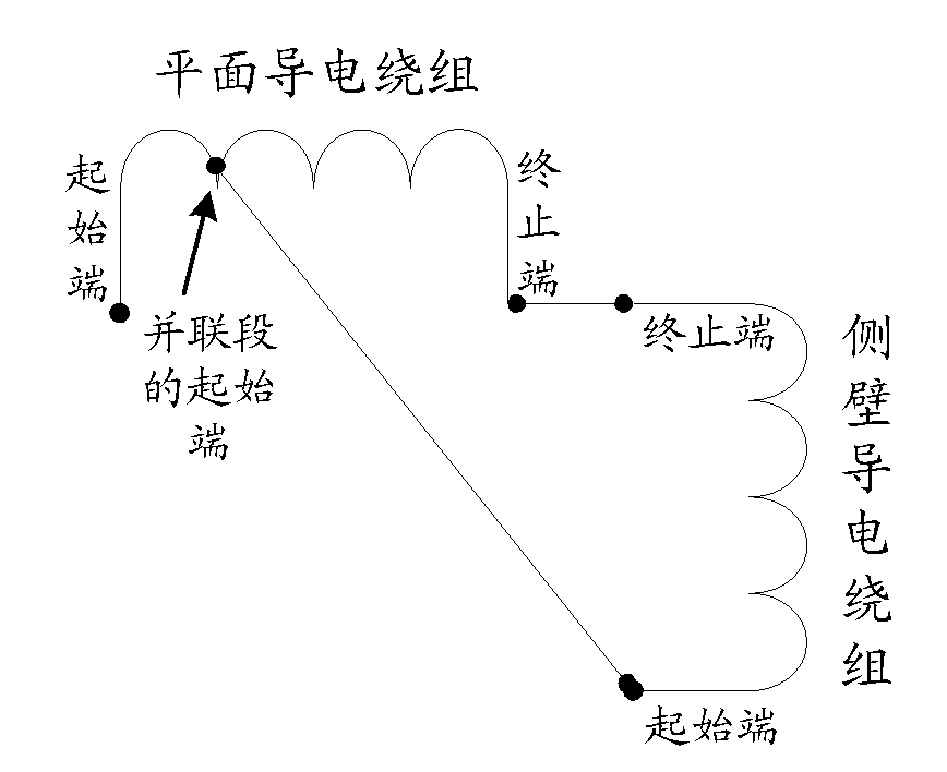
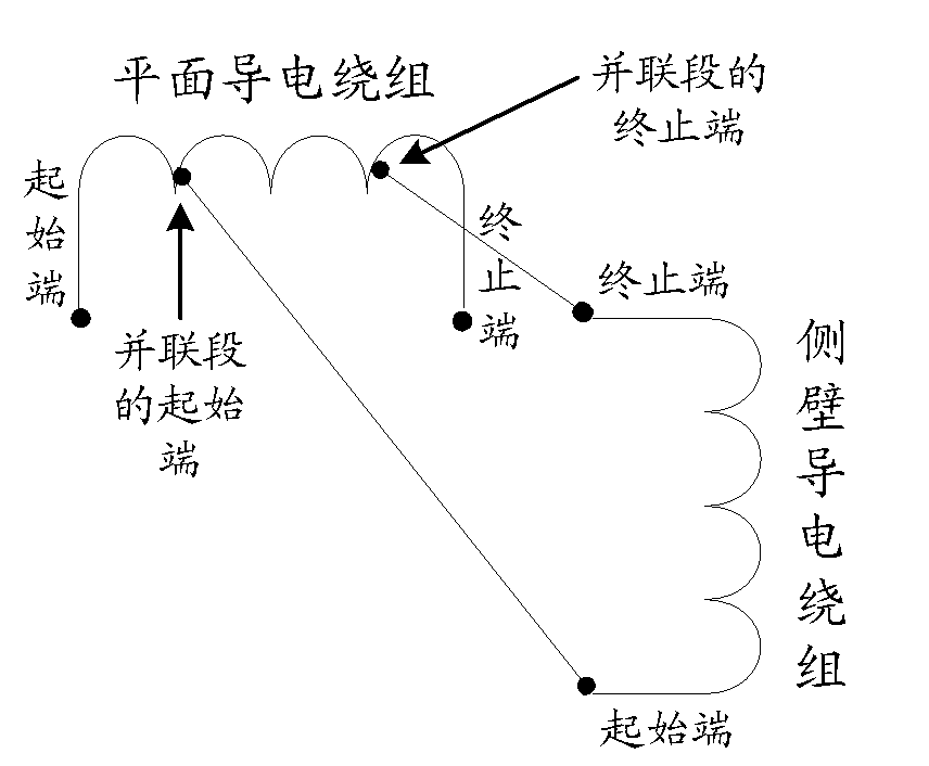
[0054]An embodiment of the power supply device of the present invention may include: at least one printed circuit board, at least one magnetic core, and at least one group of semiconductor conversion units; wherein, a magnetic core slot for installing a magnetic core is opened on the printed circuit board; the printed circuit board The slot side wall of at least one magnetic core slot of the circuit board is provided with a side wall conductive winding for cooperating with the magnetic core installed in the magnetic core slot for electromagnetic transformation, wherein the side wall conductive winding is attached to the magnetic core slot Part or all of the surface of the side wall of the slot; the semiconductor conversion unit is used to cooperate with the magnetic core and the conductive winding on the side wall to convert electric energy.

[0055] Wherein, the printed circuit board of the power supply device may be a single-layer board, a double-layer board or a multi-layer ...

Embodiment 2

[0069] In order to better understand the technical solutions of the embodiments of the present invention, the structure of a power supply device including a 4-layer PCB is taken as an example below to describe as an example. It can be understood that the scene where the power supply device includes a double-layer board or a PCB with other layers can be analogized.

[0070] see Figure 5 , the power supply device provided by the embodiment of the present invention may include:

[0071] A printed circuit board 100, two pairs of magnetic cores 201 and 202, a semiconductor conversion unit 301, and the like.

[0072] Among them, the printed circuit board 100 is provided with a magnetic core groove for installing the magnetic core, and the two pairs of magnetic cores 201 and 202 are buckled on the magnetic core groove of the printed circuit board 100 respectively; the semiconductor conversion unit 301 is welded on (or through other electrical connection mode) on the printed circui...

Embodiment 3

[0091] The embodiment of the present invention also provides a PCB winding manufacturing method, which may include: milling slots on the printed circuit board where the magnetic core slots of the sidewall conductive windings need to be arranged to form slots that require electroplating; The wall is electroplated to form a side wall conductive winding; wherein, the side surface of the side wall conductive winding is recessed or flush with the notch edge of the magnetic slot; the side wall conductive winding is used to connect with the magnetic core installed in the magnetic core slot Cooperate with electromagnetic transformation.

[0092] If the edge of the magnetic core slot is completely overlapped with the conductive winding on the side wall (that is, it is fully covered in the plane direction of the magnetic core slot), the magnetic core slot will be formed after electroplating; Complete coincidence (that is, incomplete coverage in the plane direction of the magnetic core s...


PUM


Abstract

A power device and a method for manufacturing a printed circuit board winding are disclosed. The power device includes: at least one printed circuit board (100), at least one magnetic core (201,202), and at least one group of semiconductor transforming units (301). The printed circuit board (100) is provided with magnetic core slots for installing magnetic cores (201, 202). The side wall of at least one magnetic core slot is provided with conductive side wall windings (102, 105, 107). The conductive side wall windings carry out an electromagnetic transformation in coordination with the magnetic cores (201, 202) installed in the magnetic core slots. The conductive side wall windings adhere to part or all of the surface on the side wall of the slots. The semiconductor transforming unit (301) carries out an electrical energy transformation in coordination with the magnetic cores (201, 202) and the conductive side wall windings (102, 105, 107). The breakover impedance of the conductive windings on the printed circuit board (100) can be reduced.

Description

technical field [0001] The invention relates to the field of electronic technology, in particular to a power supply device and a method for manufacturing a winding of a printed circuit board. Background technique [0002] At present, high power density has become one of the development directions of future switching converters. To increase power density, switching converters are usually in the form of modules. [0003] The power supply can be regarded as a product form of switching converters. Switching converters include: AC to DC (AC-DC, Alternating Current-Direct Current), DC to DC (DC-DC) switching converters and AC to AC ( AC-AC) switching converter, etc. A transformer, an inductor winding, and the like in a switching converter are composed of a conductive layer of a printed circuit board (PCB, Printed Circuit Board). [0004] Due to the demand for high power density, in order to reduce the footprint of magnetic devices; for example, DC-DC switching converters are al...

Claims


Application Information

Patent Timeline
Patent Type & Authority Patents(China)
IPC IPC(8): H02M1/00H05K1/11H05K1/16H05K3/40H01F5/00
CPCH05K2201/086H05K1/165H01F2027/2819
Inventor 侯召政毛恒春傅电波黄良荣陈严
Owner HUAWEI TECH CO LTD
Why Eureka
Try Eureka