A double buffer layer lateral epitaxial growth method for improving LED brightness

A technology of lateral epitaxial growth and double buffer layers, applied in the direction of electrical components, circuits, semiconductor devices, etc., can solve the problems of complex process, time-consuming samples, secondary pollution, etc., achieve simple process, reduce absorption, increase overall reflection effect

Inactive Publication Date: 2017-05-17
西安明德理工学院
View PDF7 Cites 0 Cited by
  • Summary
  • Abstract
  • Description
  • Claims
  • Application Information

AI Technical Summary

Problems solved by technology

However, the traditional lateral epitaxy method has complex process, time-consuming secondary epitaxy process and easy to cause secondary contamination of samples during operation, so it has not been effectively used in industrial production.

Method used


Image

  • A double buffer layer lateral epitaxial growth method for improving LED brightness
  • A double buffer layer lateral epitaxial growth method for improving LED brightness
  • A double buffer layer lateral epitaxial growth method for improving LED brightness

Examples


Embodiment 1

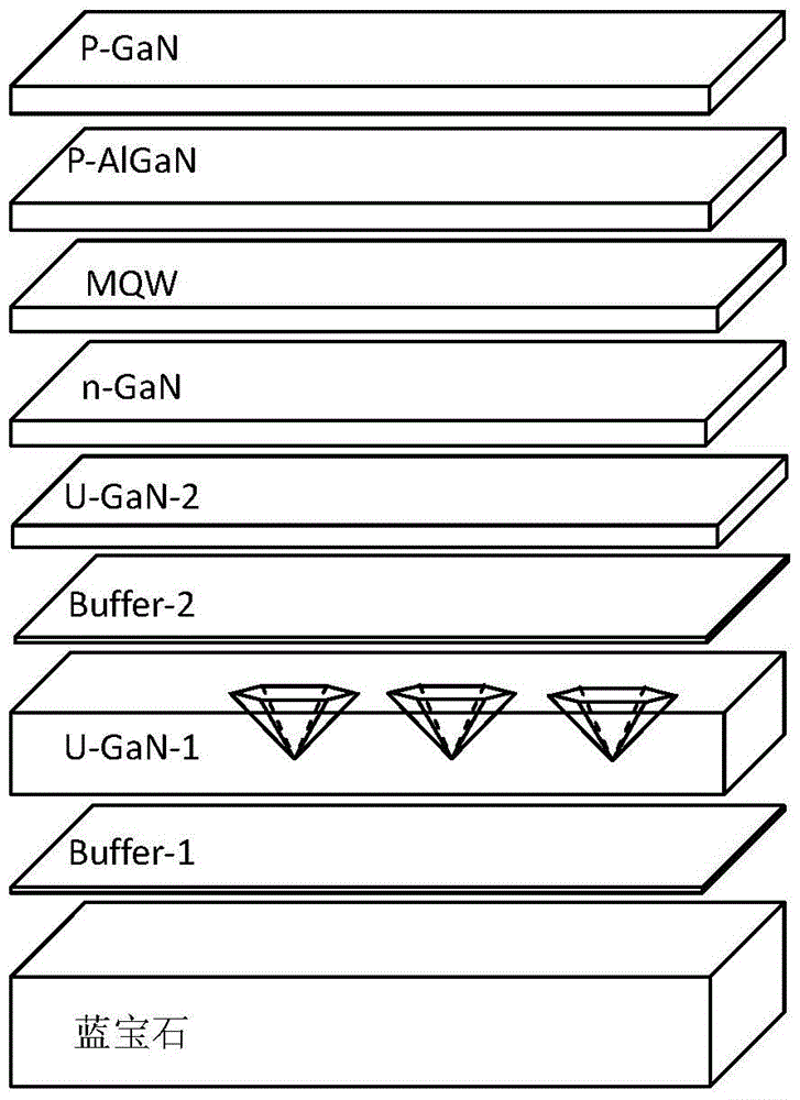
[0025] 1. Put the cleaned sapphire substrate into the MOCVD equipment and bake it at 1100°C for 10 minutes.

[0026] 2. A low-temperature buffer-1 layer with a thickness of 20nm is grown at a temperature of 520°C, and the growth pressure is 500torr.

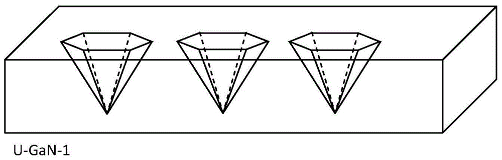
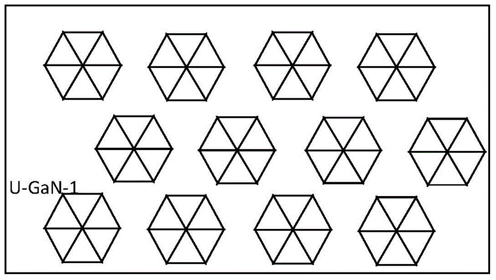
[0027] 3. Raise the temperature to 1050°C to grow a layer of undoped U-GaN-1 layer with a thickness of about 2.0um, and the growth pressure is 100torr.

[0028] 4. In the NH3 environment, raise the temperature to 1170°C, anneal for 5 minutes, and the pressure is 200torr.

[0029] 5. Lower the temperature to 650°C to grow a low-temperature buffer-2 layer with a thickness of 20nm and a growth pressure of 500torr.

[0030] 6. Then raise the temperature to 1160°C to grow a layer of undoped U-GaN-2 layer with a thickness of about 1.0um, and the growth pressure is 100torr.

[0031] 7. Raise the temperature to 1170°C, grow a layer of n-GaN doped with silane with a thickness of 2.0um, and grow at a growth pressure of 100torr.

[0032]...

Embodiment 2

[0038] 1. Put the cleaned sapphire substrate into the MOCVD equipment and bake it at 1100°C for 10 minutes.

[0039] 2. Lower the temperature to 650°C to grow a low-temperature buffer-2 layer with a thickness of 20nm and a growth pressure of 500torr.

[0040] 3. Then raise the temperature to 1160°C to grow a layer of undoped U-GaN-2 layer with a thickness of about 1.0um, and the growth pressure is 100torr.

[0041] 4. Raise the temperature to 1170° C., grow a layer of n-GaN doped with silane with a thickness of 2.0 um, and grow at a growth pressure of 100 torr.

[0042] 5. Switch the carrier gas from hydrogen to nitrogen at a pressure of 100 torr to grow multiple quantum well layers.

[0043] 6. Switch the carrier gas from nitrogen to hydrogen, and grow a p-type AlGaN layer with a thickness of 20nm and a growth pressure of 100torr at a temperature of 1185°C and 150torr.

[0044]7. The temperature is 1080°C, a layer of p-type GaN doped with Mg is grown with a thickness of 150...


PUM


Abstract

The invention discloses a transverse epitaxial growth method for double buffer layers for improving the brightness of an LED (Light Emitting Diode). The method comprises the following steps: 1) growing a first AlxGa1-xN buffer layer at a low temperature by using conical PSS (Polysaccharide Sulfate) as a growth substrate, wherein 0<=x<=1; 2) growing a first U-GaN layer with hexagonal conical array micro pits at a high temperature; 3) performing high-temperature annealing in an NH3 environment, then cooling to a low temperature, and growing a second low-temperature AlxGa1-xN buffer layer; 4) growing a second U-GaN layer at a high temperature to completely cover the hexagonal conical array micro pits of the first U-GaN layer, and forming cavities at the micro pits; 5) sequentially growing a SiH4-doped n-GaN layer, a multi-quantum well active layer, a doped p-type AlGaN barrier layer and a doped p-type GaN layer; and 6) annealing in nitrogen. According to the method, a layer of hexagonal conical array micro pits is grown on the sapphire substrate, and the buffer-2 is grown on the GaN in the area, namely GaN is grown on the GaN substrate, so that crystal nuclei with fewer defects, lower internal stress and lower crystal orientation difference can be obtained.

Description

technical field [0001] The invention belongs to the field of semiconductor electronic information, in particular to a new LED epitaxial growth method. Background technique [0002] GaN-based LED light-emitting diodes have become the third generation of high-efficiency solid-state light sources after incandescent lamps and energy-saving lamps due to their long service life, strong safety and reliability, energy saving and environmental protection. LEDs have been widely used in traffic lights, automobile tail lights, and advertising displays. Video screen, mobile phone TV backlight and white lighting field, the application prospect is very broad. At present, MOCVD equipment is mostly used to grow GaN-based LEDs on sapphire substrates. However, there is a large mismatch (16%) in the lattice constants of sapphire substrates and GaN materials, resulting in up to 10% of the GaN epitaxial film. 9- 10 10 cm –2 High linear dislocation density, high linear dislocation density will ...

Claims


Application Information

Patent Timeline
Patent Type & Authority Patents(China)
IPC IPC(8): H01L33/12H01L33/00H01L33/10H01L33/22H01L33/32
CPCH01L33/005H01L33/10H01L33/12H01L33/22H01L33/32H01L2933/0025
Inventor 张璐商毅博于春丽邹丹李渝
Owner 西安明德理工学院
Why Eureka
Try Eureka