Method for preparing antireflective film of polycrystalline silicon solar cell as well as polycrystalline silicon solar cell

A technology of solar cells and anti-reflection coatings, applied in circuits, photovoltaic power generation, electrical components, etc., can solve the problems of passivating the surface and substrate of silicon wafers, difficult to solve, multiple impurities, dislocations and grain boundaries, etc. Achieve the effect of improving photoelectric conversion efficiency, reducing dislocations and grain boundaries, and increasing maximum power

Inactive Publication Date: 2011-09-14
JETION SOLAR HLDG
View PDF5 Cites 16 Cited by
  • Summary
  • Abstract
  • Description
  • Claims
  • Application Information

AI Technical Summary

Problems solved by technology

[0004] However, the polysilicon material used in polysilicon solar cells has many defects such as impurities, dislocations, and grain boundaries. The problem of reducing the carrier life of polysilicon materials caused by the above defects will eventually affect the improvement of the photoelectric conversion efficiency of polysilicon solar cells

Method used


Image

  • Method for preparing antireflective film of polycrystalline silicon solar cell as well as polycrystalline silicon solar cell
  • Method for preparing antireflective film of polycrystalline silicon solar cell as well as polycrystalline silicon solar cell
  • Method for preparing antireflective film of polycrystalline silicon solar cell as well as polycrystalline silicon solar cell

Examples


preparation example Construction

[0032] To this end, an embodiment of the present invention provides a method for preparing an anti-reflection film for a polycrystalline silicon solar cell, which includes:

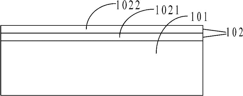
[0033] The passivation layer deposition step is used to form a passivation layer on the surface of the polysilicon wafer, specifically: feeding ammonia gas with a flow rate of 6000-9000 SCCM and silane gas with a flow rate of 800-1000 SCCM into the deposition chamber, and a radio frequency power of 3000 ~5000W, the duty ratio is 5:50, the pressure is 1500~2000mtor, and the duration is 100~300S;

[0034] The density layer deposition step is used to form a density layer on the surface of the passivation layer, specifically: feeding ammonia gas with a flow rate of 7000-9000 SCCM and silane gas with a flow rate of 400-900 SCCM into the deposition chamber, and a radio frequency power of 4500-900 SCCM 6500W, the duty ratio is 5:50, the pressure is 1500~2000mtor, and the duration is 400~600S.

[0035] The embod...

Embodiment 1

[0039] This embodiment provides a method for preparing an anti-reflection film for a polycrystalline silicon solar cell, which includes:

[0040] The passivation layer deposition step is used to form a passivation layer on the surface of the polysilicon wafer, specifically: feeding ammonia gas with a flow rate of 6000-9000 SCCM and silane gas with a flow rate of 800-1000 SCCM into the deposition chamber, and a radio frequency power of 3000 ~5000W, the duty ratio is 5:50, the pressure is 1500~2000mtor, and the duration is 100~300S.

[0041] In this embodiment, the reaction principle of producing the silicon nitride of the passivation layer is as follows:

[0042] SiH 4 +NH 3 = Si x N y h z +H 2 ;

[0043] In the passivation layer made of silicon nitride, the higher the nitrogen content, the lower the refractive index, but the poorer the passivation effect. The higher the silicon content, the better the passivation effect, but the higher the refractive index, and Light a...

Embodiment 2

[0058] This embodiment provides a specific way to form an anti-reflection film in actual production, including the following steps:

[0059] Put the graphite boat loaded with polysilicon wafers into the furnace tube in the deposition chamber of the PECVD equipment;

[0060] The deposition chamber is evacuated, a pressure test is performed, and the combustion tower is started.

[0061] Ammonia purging step: inject 2-6L of ammonia and 2-4L of nitrogen into the deposition chamber, and control the radio frequency power to 3000-5000W for 100-300S.

[0062] Vacuum the deposition chamber again, conduct a pressure test, and conduct a leak detection of the furnace tube, and wait for the temperature to reach the set value of 450°C.

[0063] Ammonia gas pre-deposition step: inject 3-6L ammonia gas into the deposition chamber, and control the radio frequency power to 3000-5000W for 100-300S.

[0064] Deposition steps of H-containing passivation layer, specific parameters: ammonia gas fl...


PUM

PropertyMeasurementUnit
thicknessaaaaaaaaaa
thicknessaaaaaaaaaa
thicknessaaaaaaaaaa

Abstract

The invention provides a method for preparing an antireflective film of a polycrystalline silicon solar cell as well as a polycrystalline silicon solar cell. The method comprises the steps of: passivation layer deposition and density layer deposition. The polycrystalline silicon solar cell comprises: a polycrystalline silicon wafer and the antireflective film located on the surface of the polycrystalline silicon wafer, wherein the antireflective film is made from silicon nitride and comprises a passivation layer and a density layer; and the passivation layer is arranged on the surface of the polycrystalline silicon wafer and the density layer is arranged on the surface of the passivation layer. In the technical scheme provided by the invention, by utilizing the passivation layer in the antireflective film, the surface of the silicon wafer and a substrate can be effectively passivated, the defects such as dislocation, crystal boundary and the like in the surface of a polycrystalline silicon material can be reduced and the carrier lifetime of the polycrystalline silicon material can be prolonged; and by utilizing the formed antireflective film, the photoelectric conversion efficiency of the polycrystalline silicon solar cell can be effectively increased and the maximum power of a cell piece is increased.

Description

Technical field: [0001] The invention relates to the technical field of solar cell manufacturing, in particular to a method for preparing an anti-reflection film for a polycrystalline silicon solar cell and the polycrystalline silicon solar cell. Background technique: [0002] With the rapid development of the economy, the demand for energy is increasing, which leads to a large shortage of energy, and at the same time causes the problem of environmental pollution to become increasingly prominent. In recent years, with the rapid development of solar energy technology, using solar cells to generate electricity has become one of the important ways to solve energy and environmental problems. Solar cells include monocrystalline silicon solar cells and polycrystalline silicon solar cells, etc. Among them, polycrystalline silicon solar cells have abundant raw materials and are relatively easy to manufacture, and their production and usage have exceeded other types of solar cells, o...

Claims


Application Information

Patent Timeline
Patent Type & Authority Applications(China)
IPC IPC(8): H01L31/18H01L31/0216H01L31/04C23C16/34
CPCY02E10/50Y02P70/50
Inventor 钱明星郭建东樊选东罗军赵静
Owner JETION SOLAR HLDG
Why Eureka
Try Eureka