Gallium nitride (GaN) based personal identification number (PIN) detector based on imaging sapphire substrate and preparation method

A patterned sapphire and ultraviolet detector technology, applied in the field of ultraviolet detectors, can solve the problems of ultraviolet detectors that have not been reported publicly, and achieve the effects of small defect density, small dark current and stable performance

Inactive Publication Date: 2012-07-18
SHANGHAI INST OF TECHNICAL PHYSICS - CHINESE ACAD OF SCI
View PDF2 Cites 14 Cited by
  • Summary
  • Abstract
  • Description
  • Claims
  • Application Information

AI Technical Summary

Problems solved by technology

[0004] At present, there is no public report on the ultraviolet detector

Method used


Image

  • Gallium nitride (GaN) based personal identification number (PIN) detector based on imaging sapphire substrate and preparation method
  • Gallium nitride (GaN) based personal identification number (PIN) detector based on imaging sapphire substrate and preparation method

Examples


Embodiment Construction

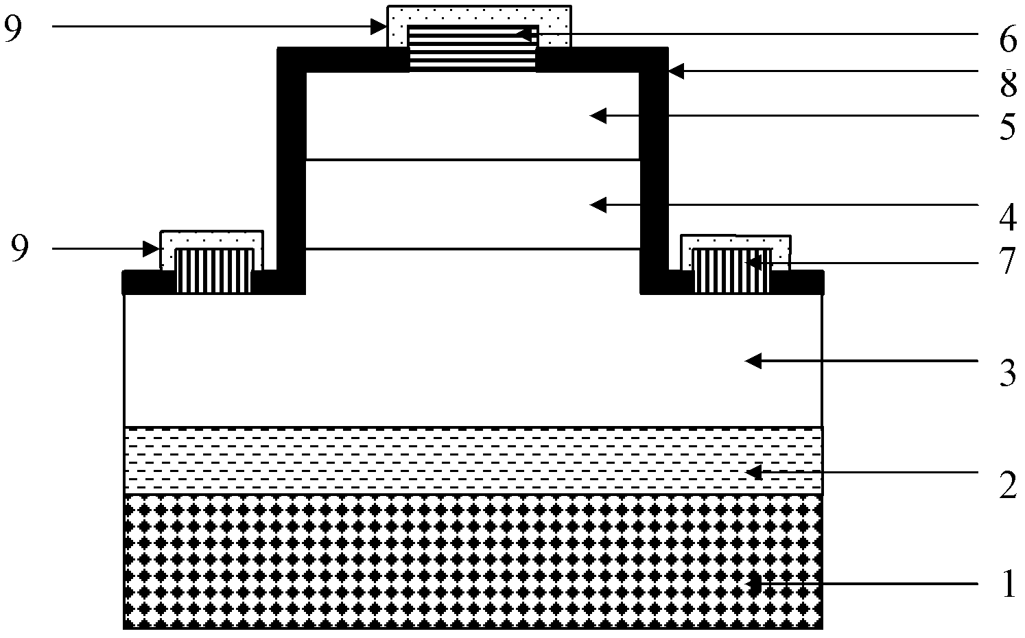
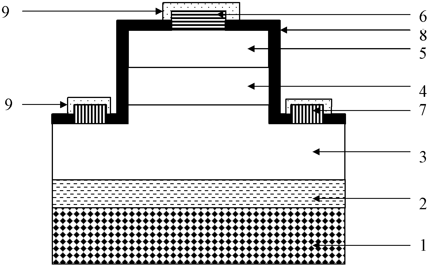
[0019] Below in conjunction with accompanying drawing and specific example of description, the fabrication process of the GaN-based PIN structure ultraviolet detector based on patterned sapphire substrate of the present invention is described in detail:

[0020] Step 1: Deposit GaN thin film material on patterned sapphire substrate 1, and grow buffer layer 2, n + GaN material layer 3, intrinsic GaN material layer 4, and p-type GaN material layer 5, wherein buffer layer growth includes low-temperature buffer layer growth, recrystallization, three-dimensional growth and two-dimensional growth;

[0021] Step 2: Epitaxial wafer cleaning, first place the epitaxial wafer in chloroform solution for ultrasonic cleaning for 10 minutes, then use chloroform, ether, acetone, and ethanol to clean the epitaxial wafer successively, each step is cleaned for 4-5 minutes, and after cleaning, use N 2 blow dry;

[0022] Step 3: Soak the sample in HF acid for 8 minutes to remove surface oxides, ...


PUM

PropertyMeasurementUnit
Thicknessaaaaaaaaaa
Electron concentrationaaaaaaaaaa
Thicknessaaaaaaaaaa

Abstract

The invention relates to a gallium nitride (GaN) based personal identification number (PIN) detector based on an imaging sapphire substrate and a preparation method. The structure is that a thick cushion layer grows on the imaging sapphire substrate, the thick cushion layer comprises low temperature cushion layer growing, recrystallization, three-dimensional growing and two-dimensional growing, and a GaN film material with good quality is obtained. An n+ type GaN layer, an intrinsic GaN layer and a p type GaN layer sequentially grow. A p ohmic contact electrode is deposited on the surface of a p layer, a p type film layer and an intrinsic layer are etched to an n+ type film layer, the shape of an etching table face is round, square or hexagon, an n type ohmic contact electrode is deposited on an n+ type layer, and an n type electrode is annular or square. A passivation layer grows and holes are drilled, the p electrode and the n electrode are exposed out, and a thickening electrode grows on the p electrode and the n electrode respectively. Devices prepared by using the method are high in growth material quality, small in dislocation and defect density, small in dark current and stable in performance. The dark current under reversal biasing voltage almost has no change, and quantum efficiency is substantially improved.

Description

technical field [0001] The invention relates to ultraviolet detector technology, in particular to an ultraviolet detector based on a GaN-based PIN structure grown on a patterned sapphire substrate (PSS, Patterned Sapphire Substrate) and a preparation method thereof. Background technique [0002] In recent years, GaN-based materials have become mainstream materials and research hotspots in the field of blue lasers and ultraviolet detectors due to their characteristics of direct bandgap semiconductors, stable chemical properties, adjustable bandgap, and wide spectral response range. GaN-based LEDs have great application prospects in energy saving; and the use of GaN-based semiconductor detectors instead of vacuum tubes for ultraviolet detection also has a significant application background; at present, ultraviolet detection also has broad application prospects in the military. [0003] Due to the mismatch between the lattice constant and thermal expansion coefficient of the sa...

Claims


Application Information

Patent Timeline
IPC IPC(8): H01L31/105H01L31/0352H01L31/18
CPCY02P70/50
Inventor 刘福浩许金通李向阳王荣阳刘秀娟陶利友刘诗嘉孙晓宇
Owner SHANGHAI INST OF TECHNICAL PHYSICS - CHINESE ACAD OF SCI
Why Eureka
Try Eureka