

Silicon carbide single crystal wafer and manufacturing method for same
a single crystal wafer and silicon carbide technology, applied in the direction of crystal growth process, polycrystalline material growth, transportation and packaging, etc., can solve the problems of deteriorating device performance, screw dislocation, screw dislocation, etc., to reduce the dislocation density of screw dislocation, reduce the occurrence of micropipes, and reduce the pressure
- Summary
- Abstract
- Description
- Claims
- Application Information
AI Technical Summary
Benefits of technology
Problems solved by technology
Method used
Image

Examples
examples
[0096]Hereinafter, the present invention will be described in more detail with reference to Examples and the like. The present invention is not limited the content of the Examples below.
example a
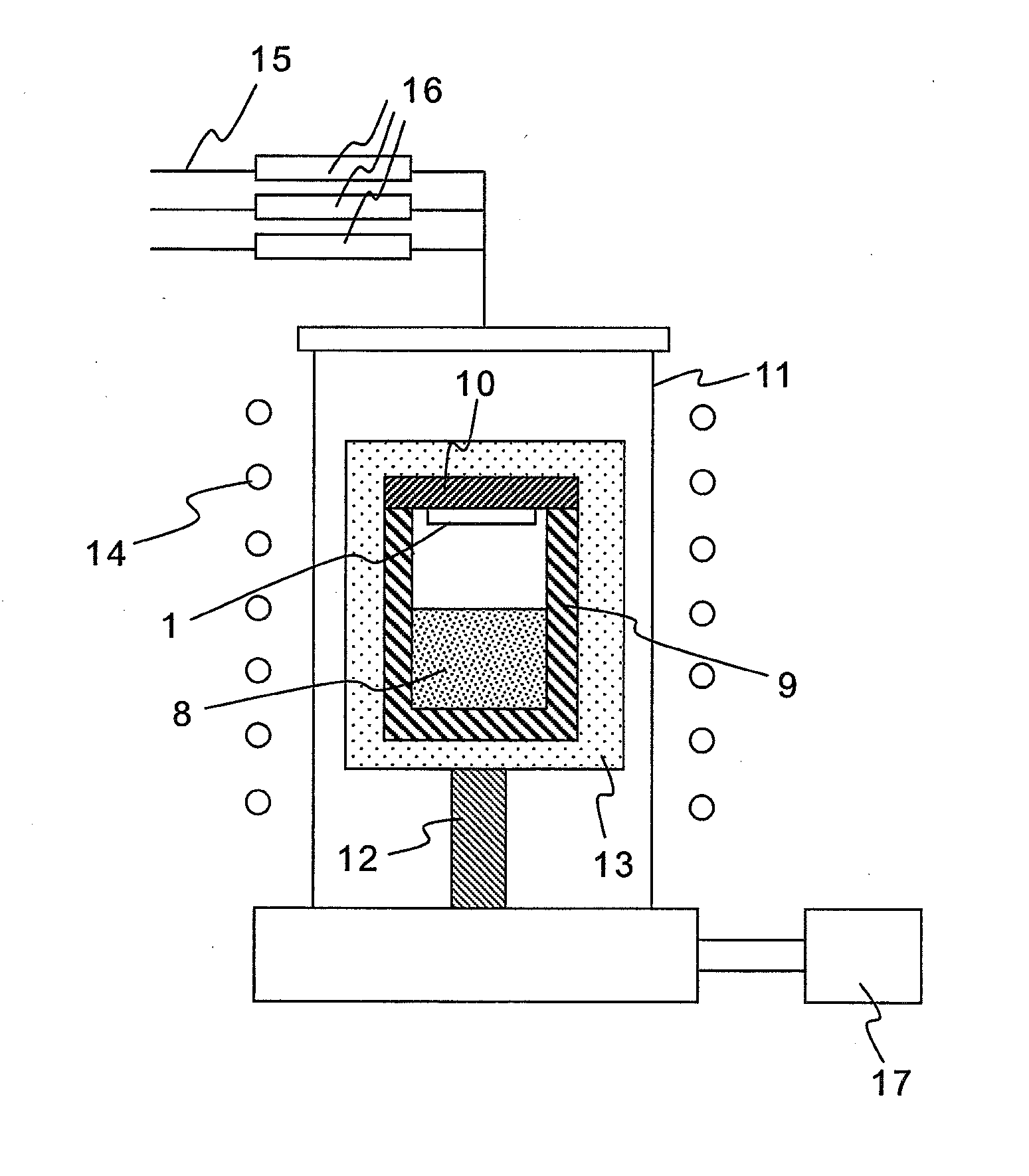
[0097]FIG. 4 depicts one example of an apparatus for growing a single crystal by a modified Lely Method (the PVT method), which is an apparatus for manufacturing a bulk SiC single crystal used to obtain a SiC single crystal substrate according to an Example of the present invention. Crystal is grown by sublimating a SiC sublimation raw material 8 by induction heating to recrystallize on a SiC seed crystal 1. The seed crystal 1 is attached onto an inner surface of a graphite lid 10, and the sublimation raw material 8 is filled in a graphite crucible 9. The graphite crucible 9 and the graphite lid 10 are covered with a graphite felt for thermal shielding and disposed on a graphite supporting rod 12 inside a double quartz tube 11. The inside of the double quartz tube 11 is vacuum evacuated by a vacuum pumping device 17 and then high purity Ar gas or nitrogen gas is flown therein through a pipe 15 while controlling by a mass flow controller 16. While regulating pressure in the quartz tu...
example a1
[0098]First, a 4H type SiC single crystal substrate having a main surface of a (0001) plane with a diameter of 75 mm and having an off angle inclined by 4 degrees in the (11-20) direction was cut from a SiC single crystal obtained in advance. The substrate was subjected to mirror surface polishing to prepare a seed crystal. The seed crystal 1 was attached to the inner surface of the graphite lid 10 of the apparatus for growing a single crystal described above and placed in the graphite crucible 9 filled with the sublimation raw material 8, and the crucible was covered with a graphite felt 13. The seed crystal 1 was mounted on the graphite supporting rod 12 and installed inside the double quartz tube 11.
[0099]Then, after vacuum evacuating the inside of the double quartz tube 11, high purity Ar gas as an atmosphere gas was flown therein, and while maintaining the pressure in the quartz tube at 80 kPa, the temperature of the seed crystal 1 was increased up to 2200° C. The pressure was ...
PUM
| Property | Measurement | Unit |
|---|---|---|
| temperature | aaaaa | aaaaa |
| temperature | aaaaa | aaaaa |
| thickness | aaaaa | aaaaa |
Abstract
Description
Claims
Application Information