Growing method for light-emitting diode epitaxial wafer

A technology of light-emitting diodes and growth methods, which is applied in the field of growth of light-emitting diode epitaxial wafers, can solve the problems of low active layer growth temperature, unfavorable active layer growth, and high growth temperature, so as to reduce defect density, reduce electron return flow, and improve The Effect of Compounding Chances

Active Publication Date: 2017-05-03
HC SEMITEK ZHEJIANG CO LTD
View PDF6 Cites 15 Cited by
  • Summary
  • Abstract
  • Description
  • Claims
  • Application Information

AI Technical Summary

Problems solved by technology

[0005] The growth temperature of the active layer is low (below 1000°C), and the growth temperature of the N-type GaN layer is high (above 1000°C), which is not conducive to the growth of the active layer

Method used


Image

  • Growing method for light-emitting diode epitaxial wafer
  • Growing method for light-emitting diode epitaxial wafer

Examples


Embodiment

[0026] An embodiment of the present invention provides a method for growing a light-emitting diode epitaxial wafer. In this embodiment, Veeco K465i or C4 metal organic compound chemical vapor deposition (English: Metal Organic Chemical VaporDeposition, referred to as: MOCVD) equipment is used to realize the LED epitaxial wafer. growth. Using high-purity hydrogen (H 2 ) or high-purity nitrogen (N 2 ) or high purity H 2 and high purity N 2 The mixed gas as the carrier gas, high-purity NH 3 As nitrogen source, trimethylgallium (TMGa) and triethylgallium (TEGa) as gallium source, trimethylindium (TMIn) as indium source, trimethylaluminum (TMAl) as aluminum source, silane (SiH4) as N-type dopant, magnesium dicene (CP 2 Mg) as a P-type dopant. The pressure of the reaction chamber is controlled at 100-600 torr.

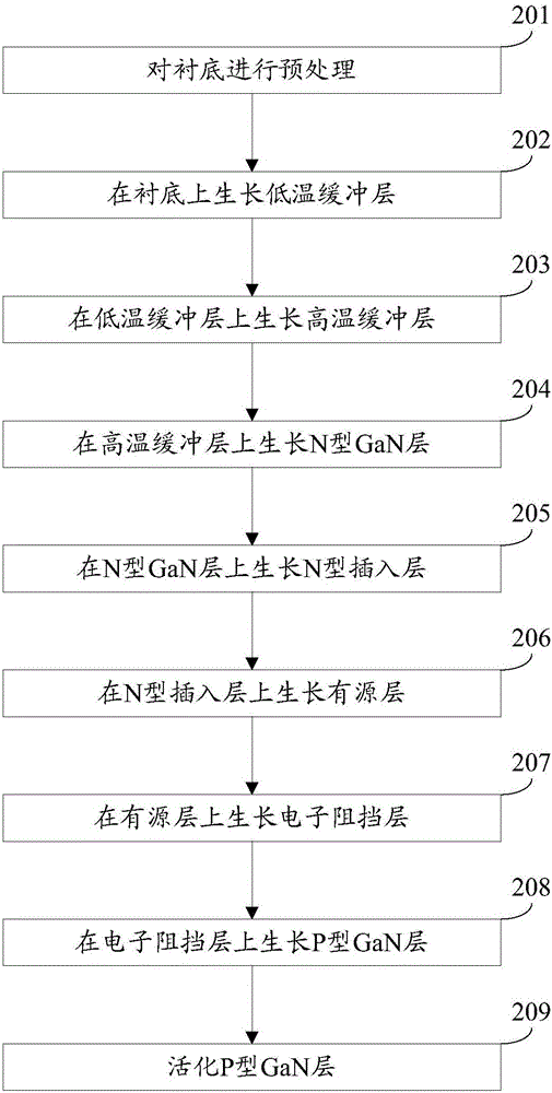
[0027] Specifically, see figure 1 , the growth method includes:

[0028] Step 201: Perform pretreatment on the substrate.

[0029] In this embodiment, the substrat...


PUM


Abstract

The invention discloses a growing method for a light-emitting diode epitaxial wafer, and belongs to the technical field of semiconductors. The growing method comprises the following steps: growing a low-temperature buffer layer, a high-temperature buffer layer, an N-type GaN layer, an N-type inserting layer, an active layer, an electron barrier layer and a P-type GaN layer in sequence on a substrate, wherein the growth temperature of the N-type GaN layer is greater than that of the N-type inserting layer which is greater than that of the active layer; the N-type inserting layer comprises a first sublayer, a second sublayer and a third sublayer which are laminated in sequence; the first sublayer is a superlattice structure formed by alternately laminating two GaN layers in which the doping concentrations of the N-type doping agents are different, and the doping concentration of the N-type doping agent in the first sublayer is smaller than that of the N-type doping agent in the N-type GaN layer; the second sublayer is an AlGaN layer or a superlattice structure formed by alternately laminating at least three AlGaN layers and at least three GaN layers; and the third sublayer is an InGaN layer. The N-type inserting layer in the invention plays a buffer role, and is beneficial for the growth of the active layer.

Description

technical field [0001] The invention relates to the technical field of semiconductors, in particular to a method for growing a light-emitting diode epitaxial wafer. Background technique [0002] A light-emitting diode (English: Light Emitting Diode, referred to as: LED) is a semiconductor electronic component that can emit light. As an efficient, environmentally friendly, and green new solid-state lighting source, LEDs are rapidly and widely used in traffic lights, automotive interior and exterior lights, urban landscape lighting, and mobile phone backlights. [0003] An existing LED epitaxial wafer includes a substrate, and a low-temperature buffer layer, a high-temperature buffer layer, an N-type GaN layer, an active layer, and a P-type GaN layer sequentially stacked on the substrate. [0004] In the process of realizing the present invention, the inventor finds that there are at least the following problems in the prior art: [0005] The growth temperature of the active...

Claims


Application Information

Patent Timeline
Patent Type & Authority Applications(China)
IPC IPC(8): H01L33/00H01L33/12H01L33/04H01L33/14H01L33/06
CPCH01L33/007H01L33/04H01L33/06H01L33/12H01L33/14
Inventor 姚振从颖胡加辉
Owner HC SEMITEK ZHEJIANG CO LTD
Why Eureka
Try Eureka