

Non-contact glass micro-nano structure processing method
A processing method and non-contact technology, applied in the field of preparing micro-nano structures, can solve the problems of harsh etching line width and expensive patterning, and achieve the effect of simplifying the process cost
- Summary
- Abstract
- Description
- Claims
- Application Information
AI Technical Summary
Problems solved by technology
Method used
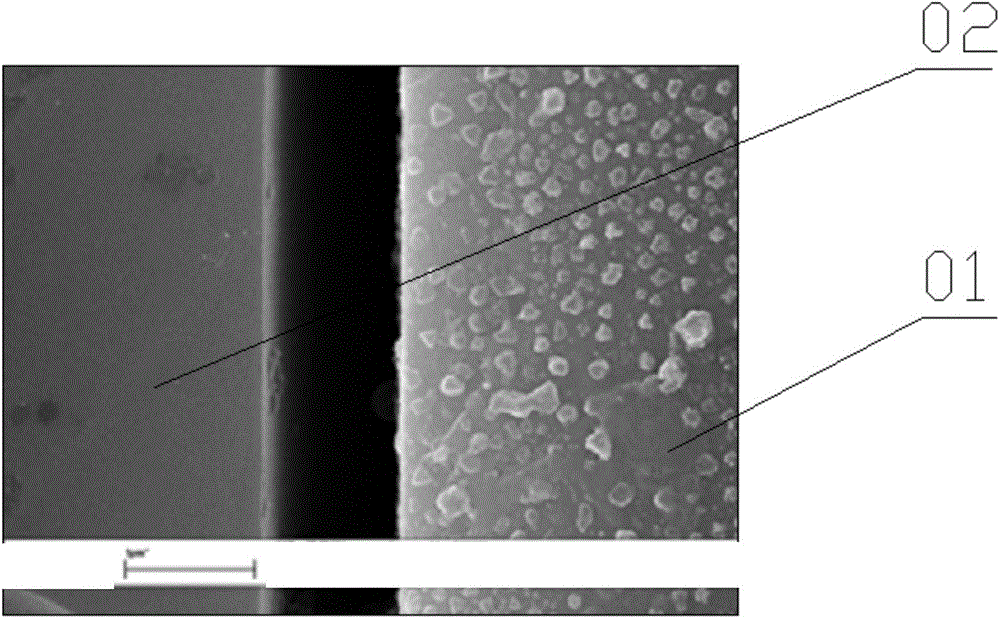
Image

Examples
Embodiment Construction
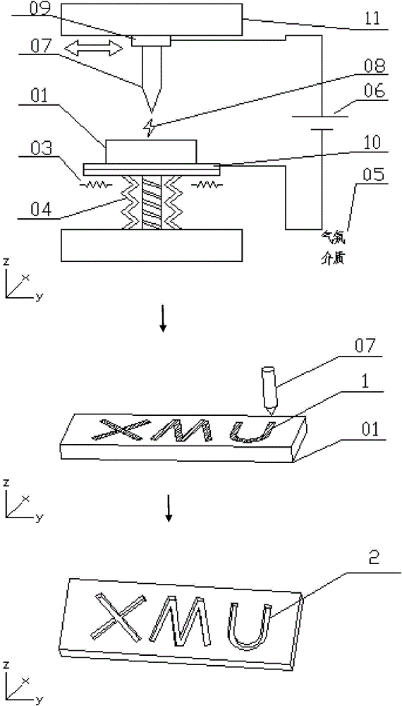
[0018] see figure 1 , the specific steps of the embodiment of the present invention are given below:
[0019] Step 1: The glass sheet 01 is placed on the Z-axis mobile platform 04 and connected to the negative pole of the power supply 06; the conductive material 07 is made of semiconductor silicon material, processed into a needle-like shape by micro-nano etching technology, and the conductive material 07 is placed on the glass sheet 01 , fixed on the X-Y plane mobile platform 11, and connected to the positive pole of the power supply 06; turn on the heating device 03 to heat the glass sheet 01 to between 250°C and 500°C; change the distance value between the glass sheet 01 and the conductive material 07 a; and adjust the voltage value of the power supply 06 to U to break down the atmosphere medium 05 and form an arc 08. Taking air as an example, the distance value a between the glass sheet 01 and the conductive material 07 and the voltage value U of the power supply 06 satis...
PUM
 Abstract
Description
Claims
Application Information