Array substrate, manufacturing method thereof, and display device

An array substrate and substrate substrate technology, applied in optics, instruments, electrical components, etc., can solve the problems of high production cost and low yield rate, and achieve the effect of improving yield rate, reducing the number of times, and reducing one patterning process.

Active Publication Date: 2018-07-06
BOE TECH GRP CO LTD +1
View PDF5 Cites 0 Cited by
  • Summary
  • Abstract
  • Description
  • Claims
  • Application Information

AI Technical Summary

Problems solved by technology

[0004] However, since the number of patterning processes directly affects the production cost and the yield rate, that is, the more the patterning process, the longer the production cycle, the higher the production cost, and the lower the yield rate. Therefore, how to reduce the The number of composition processes is a technical problem that needs to be solved urgently

Method used


Image

  • Array substrate, manufacturing method thereof, and display device
  • Array substrate, manufacturing method thereof, and display device
  • Array substrate, manufacturing method thereof, and display device

Examples


Embodiment 1

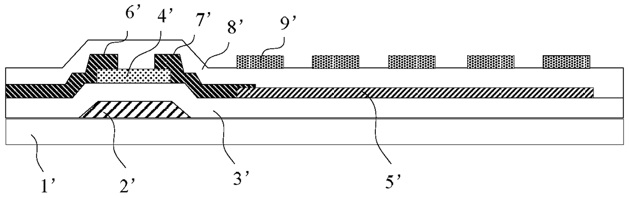
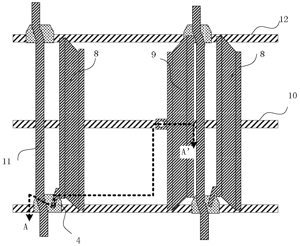
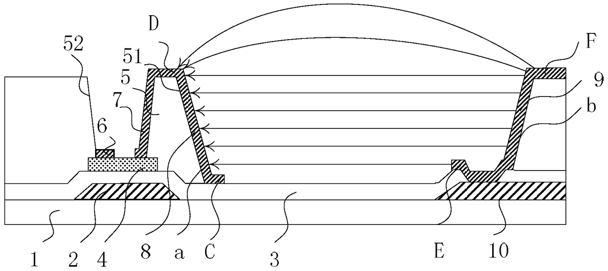
[0032] An embodiment of the present invention provides an array substrate, such as figure 2 with image 3 As shown, the array substrate includes a base substrate 1 and a gate 2 stacked on the base substrate 1, a gate insulating layer 3 and an active layer 4. The array substrate also includes a passivation layer disposed on the active layer 4. The passivation layer 5 and the source electrode 6, the drain electrode 7, the first electrode 8 and the second electrode 9 arranged on the same layer on the passivation layer 5; wherein, the first via hole 51 is arranged on the passivation layer 5, and the second via hole 51 is arranged on the passivation layer 5. A via hole 51 includes two opposite inclined sides; the first electrode 8 at least partially covers one side of the first via hole 51, the second electrode 9 at least partially covers the other side of the first via hole 51, and the second electrode 9 It is electrically connected with the common electrode lead 10; the second ...

Embodiment 2

[0047] An embodiment of the present invention provides a method for manufacturing an array substrate, such as Figure 4 shown, including:

[0048] In step 401, a pattern including a gate is formed on the base substrate through a first patterning process. Exemplarily, a conductive layer is formed on the base substrate by methods such as plasma-enhanced chemical vapor deposition, sputtering or thermal evaporation, a photoresist is coated on the conductive layer, and a mask plate with a grid pattern is used Covering the conductive layer coated with photoresist, after exposure, development, etching and other steps, a pattern including the gate is formed.

[0049] Step 402 , forming a gate insulating layer on the base substrate formed with a pattern including a gate. Exemplarily, the gate insulating layer is formed on the base substrate on which the pattern including the gate is formed by plasma enhanced chemical vapor deposition, sputtering or thermal evaporation.

[0050] In s...


PUM

PropertyMeasurementUnit
thicknessaaaaaaaaaa

Abstract

The invention discloses an array substrate, a manufacturing method thereof, and a display device, which relate to the field of display technology and can reduce the number of patterning processes used in the preparation process of the array substrate. Wherein, the array substrate includes a base substrate and a gate stacked on the base substrate, a gate insulating layer and an active layer, and also includes a passivation layer disposed on the active layer and a passivation layer disposed on the passivation layer. The source electrode, the drain electrode, the first electrode and the second electrode are arranged in the same layer; the passivation layer is provided with a first via hole, and the first via hole includes two opposite inclined sides; the first electrode at least partially covers the second electrode One side of a via hole, the second electrode at least partially covers the other side of the first via hole, the second electrode is electrically connected to the common electrode lead; a second via hole is also provided on the passivation layer, and the source and drain pass through The second via hole is connected to the active layer, and the first electrode is electrically connected to the source or the drain. The array substrate provided by the present invention can be applied to display devices.

Description

technical field [0001] The present invention relates to the field of display technology, in particular to an array substrate, a manufacturing method thereof, and a display device. Background technique [0002] Advanced-Super Dimensional Switching (abbreviation: ADS) display technology forms a multi-dimensional electric field through the electric field generated at the edge of the slit electrode in the same plane and the electric field generated between the slit electrode layer and the plate electrode layer, so that the liquid crystal All aligned liquid crystal molecules between the slit electrodes in the cell and above the slit electrodes can be rotated, thereby improving the working efficiency of the liquid crystal. [0003] Generally, a display device adopting ADS display technology includes an array substrate, such as figure 1 As shown, the array substrate includes a base substrate 1' and a gate electrode 2', a gate insulating layer 3', an active layer 4', a pixel electr...

Claims


Application Information

Patent Timeline
Patent Type & Authority Patents(China)
IPC IPC(8): G02F1/13G02F1/1362
CPCG02F1/1303G02F1/1362G02F1/136231G02F1/134309G02F1/134363G02F1/136227H01L27/124H01L27/1248H01L29/41733
Inventor 张鹏举杜晓健徐斌
Owner BOE TECH GRP CO LTD
Why Eureka
Try Eureka