
Method for electroplating laminated ZnO pressure-sensitive ceramic resistor chip

A pressure-sensitive ceramic and electroplating technology, applied in resistors, resistor manufacturing, circuits, etc., can solve problems such as damage to the organic insulating protective layer, organic insulating layer failure, device disconnection, etc., to achieve good moisture and dust resistance, The effect of avoiding the phenomenon of creeping plating and preventing deterioration

Inactive Publication Date: 2015-09-30
XI'AN POLYTECHNIC UNIVERSITY
View PDF6 Cites 1 Cited by
  • Summary
  • Abstract
  • Description
  • Claims
  • Application Information

AI Technical Summary

Problems solved by technology

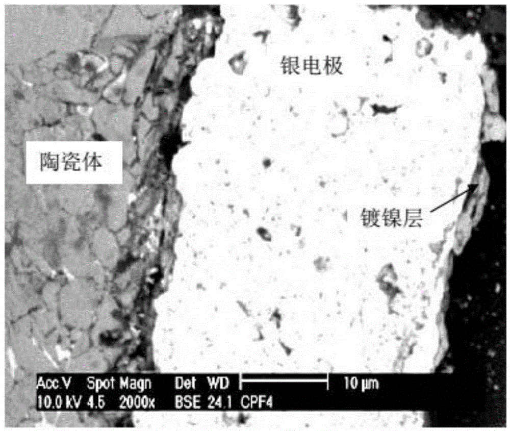
[0006] (1) Due to the wrapping of the organic insulating material on the silver electrode, the device is easily disconnected and fails;
[0007] (2) In order to improve the uniformity of electroplating, the laminated chip device is placed in the rotating electroplating tank during the electroplating process. Due to the friction between the devices, the soft organic insulating protective layer on the surface is easily damaged, resulting in creep plating;
[0008] (3) When the ceramic body of the laminated chip device is a semiconductor ceramic, a large current will flow through the laminated chip device during the electroplating process, and the heating process will easily lead to the failure of the organic insulating layer on the surface of the ceramic body

Method used


Image

  • Method for electroplating laminated ZnO pressure-sensitive ceramic resistor chip

Examples


Embodiment 1

[0109] Take the laminated ZnO ceramic sheet with a rectangular cross section for sintering treatment to obtain the sintered laminated ZnO ceramic sheet; put the corundum and the sintered laminated ZnO ceramic sheet in the drum together, and the corundum The mass ratio to the sintered laminated ZnO ceramic sheet is 2:1; start the drum to rotate, so that the emery in the drum and the sintered laminated ZnO ceramic sheet are mixed and tumbled, and the mixed tumbler is controlled The time is: 20min, in the process of mixing and tumbling, use emery to polish the outer surface of the sintered laminated ZnO ceramic sheet to obtain a laminated ZnO ceramic sheet with a smooth outer surface;

[0110] Place the laminated ZnO ceramic sheet with a smooth outer surface in an ultrasonic cleaner, and add deionized water to the ultrasonic cleaner; turn on the ultrasonic cleaner, and use the ultrasonic cleaner to clean the laminated ZnO ceramic sheet for 10 minutes; The cleaned laminated ZnO ce...

Embodiment 2

[0115] Take the laminated ZnO ceramic sheet with a rectangular cross section for sintering treatment to obtain the sintered laminated ZnO ceramic sheet; put the corundum and the sintered laminated ZnO ceramic sheet in the drum together, and the corundum The mass ratio to the sintered laminated ZnO ceramic sheet is 2.5:1; start the drum to rotate, so that the emery in the drum and the sintered laminated ZnO ceramic sheet are mixed and tumbled, and the mixed tumbler is controlled The time is: 25min, in the process of mixing and tumbling, use emery to polish the outer surface of the sintered laminated ZnO ceramic sheet to obtain a laminated ZnO ceramic sheet with a smooth outer surface;

[0116] The laminated ZnO ceramic sheet with a smooth outer surface is placed in an ultrasonic cleaner, and deionized water is added to the ultrasonic cleaner; the ultrasonic cleaner is turned on, and the laminated ZnO ceramic sheet is cleaned by the ultrasonic cleaner for 20 minutes; The cleaned...

Embodiment 3

[0121] Take the laminated ZnO ceramic sheet with a rectangular cross section for sintering treatment to obtain the sintered laminated ZnO ceramic sheet; put the corundum and the sintered laminated ZnO ceramic sheet in the drum together, and the corundum The mass ratio to the sintered laminated ZnO ceramic sheet is 3:1; start the drum to rotate, so that the emery in the drum and the sintered laminated ZnO ceramic sheet are mixed and tumbled, and the mixed tumbler is controlled The time is: 30min, in the process of mixing and tumbling, use emery to polish the outer surface of the sintered laminated ZnO ceramic sheet to obtain a laminated ZnO ceramic sheet with a smooth outer surface;

[0122] The laminated ZnO ceramic sheet with a smooth outer surface is placed in an ultrasonic cleaner, and deionized water is added to the ultrasonic cleaner; the ultrasonic cleaner is turned on, and the laminated ZnO ceramic sheet is cleaned by the ultrasonic cleaner for 30 minutes; The cleaned l...


PUM

PropertyMeasurementUnit
Diameteraaaaaaaaaa
Thicknessaaaaaaaaaa
Diameteraaaaaaaaaa

Abstract

The invention discloses a method for electroplating a laminated ZnO pressure-sensitive ceramic resistor chip, which comprises the following steps: putting a sintered laminated ZnO ceramic chip and corundum into a rotating roller, and carrying mixing and barreling to obtain a laminated ZnO ceramic chip with smooth external surface; cleaning the laminated ZnO ceramic chip with smooth external surface to obtain a cleaned laminated ZnO ceramic chip; carrying out insulation treatment on the cleaned laminated ZnO ceramic chip by using an insulation treatment modification solution to obtain a laminated ZnO ceramic wafer coated with a glass insulation layer on the external surface; and sequentially carrying out silver plating and barrel plating on the laminated ZnO ceramic wafer coated with a glass insulation layer on the external surface, thereby completing the electroplating on the laminated ZnO pressure-sensitive ceramic resistor chip. The method can form a firm insulation layer on the device surface, overcomes the defect of overplating in the electroplating process, and is beneficial to inhibiting property deterioration in the device operation process.

Description

technical field [0001] The invention belongs to the technical field of preparation methods of electrical materials, and in particular relates to a method for electroplating a laminated ZnO varistor ceramic resistor. Background technique [0002] At present, the electronic products on the market are rapidly developing toward the direction of miniaturization, low voltage and low energy consumption, especially the multilayer chip devices suitable for surface mounting, such as multilayer chip varistors, which have been widely used. big development. [0003] The preparation method of the existing laminated chip device is: first adopt casting method or thick film method to prepare green body, then obtain laminated chip device after sintering and being treated by silver; In order to improve the surface mounting time of laminated chip device Solder resistance, and sometimes a layer of other metals are plated on the silver electrodes, and the metals usually used are Ni or Sn / Pb. ...

Claims


Application Information

Patent Timeline
IPC IPC(8): C25D5/54C25D3/12H01C17/00
Inventor 成鹏飞宋江
Owner XI'AN POLYTECHNIC UNIVERSITY
Learn More