Exposure device and exposure method

A technology of exposure device and exposure method, which is applied in the field of integrated circuit manufacturing, can solve the problems that the space occupied by the dual-unit structure is unaffordable for equipment users, cannot expose high-resolution graphics, and increases the demand for equipment space, so as to save stepping time , Save space and size, improve productivity

Active Publication Date: 2017-12-29
SHANGHAI MICRO ELECTRONICS EQUIP (GRP) CO LTD
View PDF12 Cites 0 Cited by
  • Summary
  • Abstract
  • Description
  • Claims
  • Application Information

AI Technical Summary

Problems solved by technology

This defect greatly limits the application of maskless lithography, making it impossible to expose high-resolution patterns, or can only be exposed at a very slow scanning speed, which greatly affects the yield
[0007] In addition, the workflow of traditional exposure equipment includes the processes of film loading, measurement, and exposure. Although the advent of the dual-stage structure makes the time of film loading and measurement not affect the yield of the equipment, it increases the demand for equipment space. The size of the circle and the substrate is getting larger and larger, and the space occupied by the double-stage structure will gradually make it difficult for equipment users to afford

Method used


Image

  • Exposure device and exposure method
  • Exposure device and exposure method
  • Exposure device and exposure method

Examples


Embodiment Construction

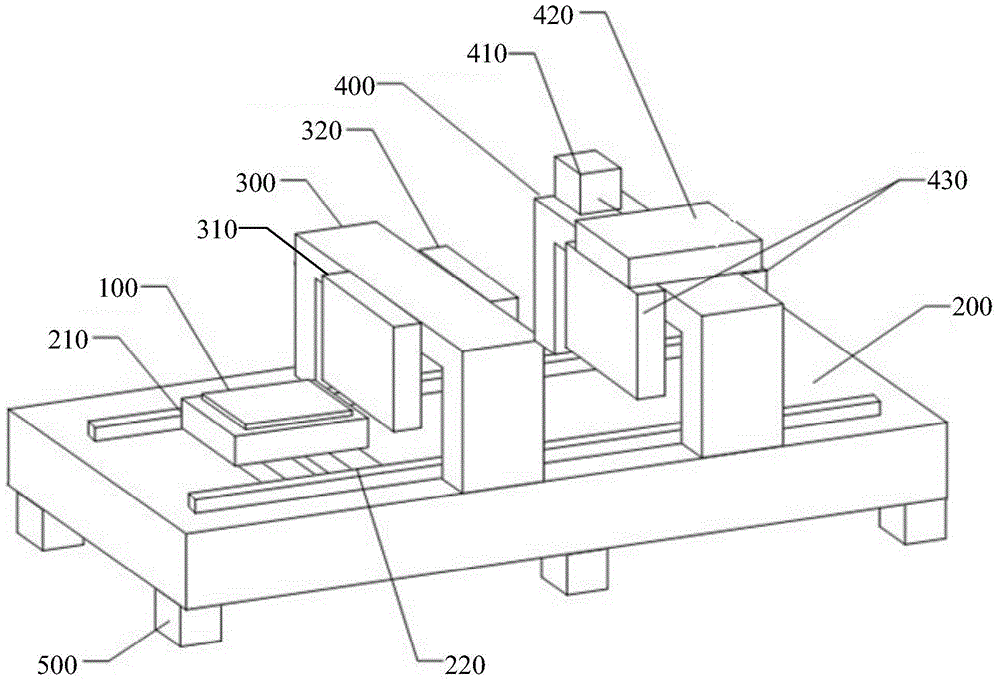
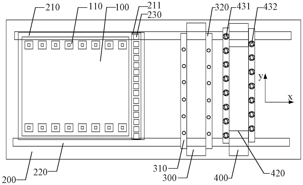
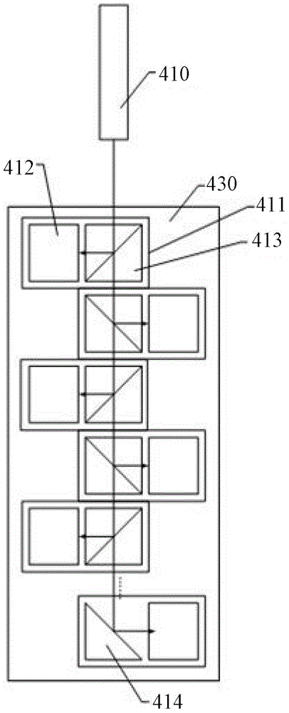
[0054] The exposure apparatus and exposure method of the present invention will be described in more detail below in conjunction with schematic diagrams, wherein preferred embodiments of the present invention are represented, it should be understood that those skilled in the art can modify the present invention described here, and still realize the advantages of the present invention Effect. Therefore, the following description should be understood as the broad knowledge of those skilled in the art, but not as a limitation of the present invention.

[0055] In the interest of clarity, not all features of an actual implementation are described. In the following description, well-known functions and constructions are not described in detail since they would obscure the invention with unnecessary detail. It should be appreciated that in the development of any actual embodiment, numerous implementation details must be worked out to achieve the developer's specific goals, such as ...


PUM


Abstract

The present invention proposes an exposure device and an exposure method. A measurement main substrate equipped with a substrate alignment system and a focusing system and an exposure main substrate equipped with an exposure system driver, an exposure system group, and a light source are added to the exposure table. The photosynchronous virtual mask imaging technology solves the contradiction between resolution and productivity that plagues maskless lithography, and achieves high productivity at high resolution; it separates scanning and stepping motions into different actuators, saving The stepping time is shortened, the productivity is optimized, and the space size of the whole machine is saved at the same time. , Alignment time is separated from lithography production, increasing productivity.

Description

technical field [0001] The invention relates to the field of integrated circuit manufacturing, in particular to an exposure device and an exposure method. Background technique [0002] The projection exposure device can project the circuit pattern on the reticle onto the substrate coated with photoresist at a certain magnification or reduction ratio through an optical system such as a projection objective lens. At present, projection exposure devices have been widely used in the manufacture of integrated circuits, and in recent years, the scope of application has been extended to fields such as flat panel display and printed circuit board manufacturing. [0003] As the market demand for semiconductor products continues to increase and manufacturers continue to pursue their price competitiveness, the size of initially processed silicon wafers, flat panel display substrates and PCB substrates continues to increase. In the field of wafer manufacturing, the demand for 450mm equ...

Claims


Application Information

Patent Timeline
Patent Type & Authority Patents(China)
IPC IPC(8): G03F7/20
Inventor 许琦欣王帆周畅
Owner SHANGHAI MICRO ELECTRONICS EQUIP (GRP) CO LTD
Why Eureka
Try Eureka