Transistor and formation method

A technology of transistors and insulating layers, applied in semiconductor devices, semiconductor/solid-state device manufacturing, electrical components, etc., to achieve the effect of improving integration and reducing substrate area

Active Publication Date: 2015-09-30
SEMICON MFG INT (SHANGHAI) CORP
View PDF3 Cites 3 Cited by
  • Summary
  • Abstract
  • Description
  • Claims
  • Application Information

AI Technical Summary

Problems solved by technology

[0004] In order to further improve the integration level of the chip, the size of the transistor is also continuously reduced with the decrease of the process node, but the short channel effect of the transistor due to the size reduction is also more and more significant
[0005] How to further improve the integration of transistors is a big challenge

Method used


Image

  • Transistor and formation method
  • Transistor and formation method
  • Transistor and formation method

Examples


Embodiment Construction

[0032] As described in the prior art, the transistors in the existing integrated circuits are arranged in a planar manner, occupying a relatively large chip area, which is not conducive to the improvement of device integration.

[0033] The study found that the columnar transistor structure is beneficial to increase the channel area of ​​the transistor and is easy to integrate.

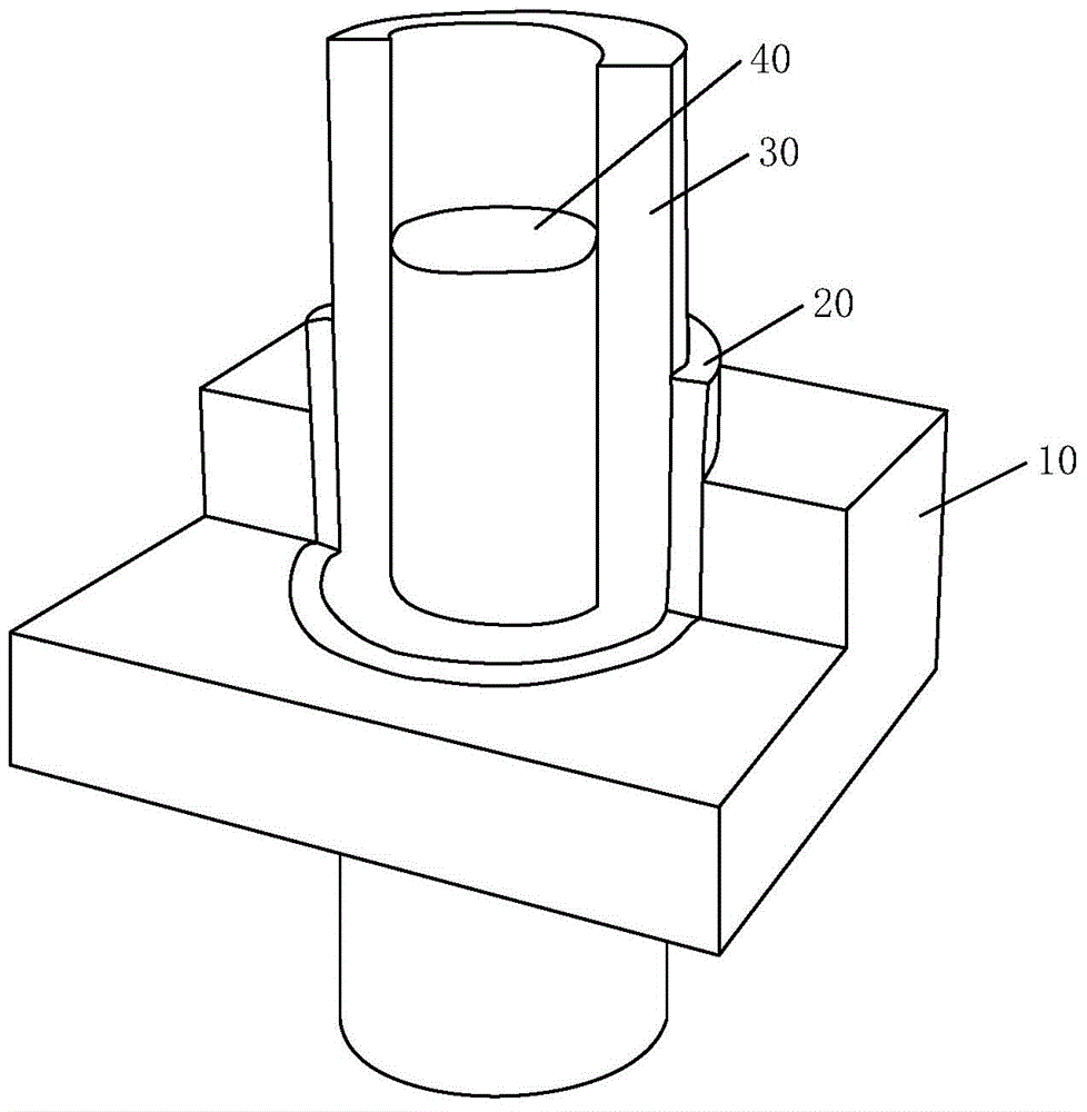
[0034] Please refer to figure 1 , which provides a schematic cross-sectional structure diagram of a columnar transistor according to an embodiment of the present invention.

[0035] The columnar transistor includes: a dielectric layer 40 at the center, a channel layer 30 surrounding and covering the surface of the dielectric layer, a gate dielectric layer 20 surrounding and covering the surface of the channel layer, and a part of the gate dielectric layer surrounding and covering 20 of the grid 10.

[0036] The channel area of ​​the columnar transistor is larger, which can increase the saturation c...


PUM


Abstract

The invention provides a transistor and a formation method thereof. The formation method of the transistor includes providing a substrate and forming a plurality of insulating layers and a plurality of fake grid layers stacked at intervals on the surface of the substrate; forming a through hole in the insulating layers and the fake grid layers, wherein the bottom of the through hole is at the surface of the substrate; forming a channel layer on the surface of the through hole; removing the fake grid layers so as to form grooves between adjacent insulating layers; forming grid medium layers on the surface of the inner wall of a grooves and the surface of the channel layer; forming grids filling the grooves and the through hole on the surfaces of the grid medium layers. By adopting the above method, integration level of the transistor can be improved.

Description

technical field [0001] The invention relates to the technical field of semiconductors, in particular to a transistor and a forming method thereof. Background technique [0002] MOS transistors are one of the core devices in modern semiconductor integrated circuits. MOS transistors usually include: a semiconductor substrate, a gate structure on the surface of the semiconductor substrate, and a source and drain in the semiconductor substrate on both sides of the gate structure. , the gate structure includes a gate dielectric layer and a gate located on the surface of the gate dielectric layer, and the doping type of the source and drain is consistent with the type of the MOS transistor. The integration level of the transistor has a great influence on the integration level of the chip. [0003] Since the existing transistors are generally planarly distributed on the substrate, the size of a single transistor has a great influence on the integration level of the chip. [0004]...

Claims


Application Information

Patent Timeline
Patent Type & Authority Applications(China)
IPC IPC(8): H01L29/78H01L29/423H01L21/336H01L21/28
Inventor 三重野文健
Owner SEMICON MFG INT (SHANGHAI) CORP
Why Eureka
Try Eureka