

Solder distribution of semiconductor device heat radiation module
Patent Information
- Authority / Receiving Office
- CN · China
- Current Assignee / Owner
- BEIJING UNIV OF TECH
- Publication Date
- 2015-10-07
Smart Images
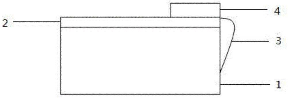
Figure 1 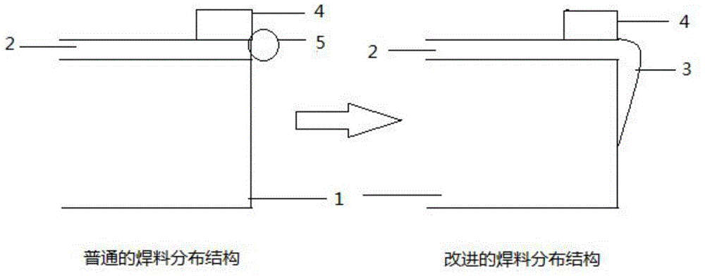
Figure 2 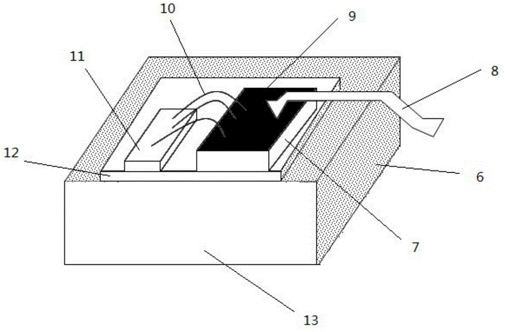
Figure 3
Abstract
Description
technical field
[0001] The invention relates to solder distribution of a heat dissipation module of a semiconductor device, belongs to the field of semiconductor device manufacturing, and relates to a preparation process of a heat dissipation module of a semiconductor device. Background technique
[0002] Semiconductor devices refer to discrete devices made of semiconductor materials. According to different semiconductor materials, different processes and geometric structures, researchers have developed a variety of semiconductor devices with different functions. These semiconductor devices are widely used in information storage, communication, military and medical fields. This requires semiconductor devices to have the characteristics of excellent performance, small size, light weight and low power consumption. In order to achieve the above goals, very high requirements are put forward for the manufacturing process of the semiconductor device heat dissipation module. [...