Radio frequency LDMOS device and manufacturing method thereof

A manufacturing method and device technology, applied in semiconductor/solid-state device manufacturing, semiconductor devices, electrical components, etc., to achieve the effects of improving frequency characteristics, reducing equivalent dielectric constant, and reducing gate-to-drain capacitance

Inactive Publication Date: 2015-10-07
UNIV OF ELECTRONICS SCI & TECH OF CHINA +1
View PDF5 Cites 0 Cited by
  • Summary
  • Abstract
  • Description
  • Claims
  • Application Information

AI Technical Summary

Problems solved by technology

However, the traditional structure is mainly to improve the influence of device parasitic capacitance on the frequency characteristics of the device and its effect has tended to be saturated, while the intrinsic gate-drain capacitance that has a greater influence on the frequency characteristics of the device cannot be reduced.

Method used


Image

  • Radio frequency LDMOS device and manufacturing method thereof
  • Radio frequency LDMOS device and manufacturing method thereof
  • Radio frequency LDMOS device and manufacturing method thereof

Examples


Embodiment 1

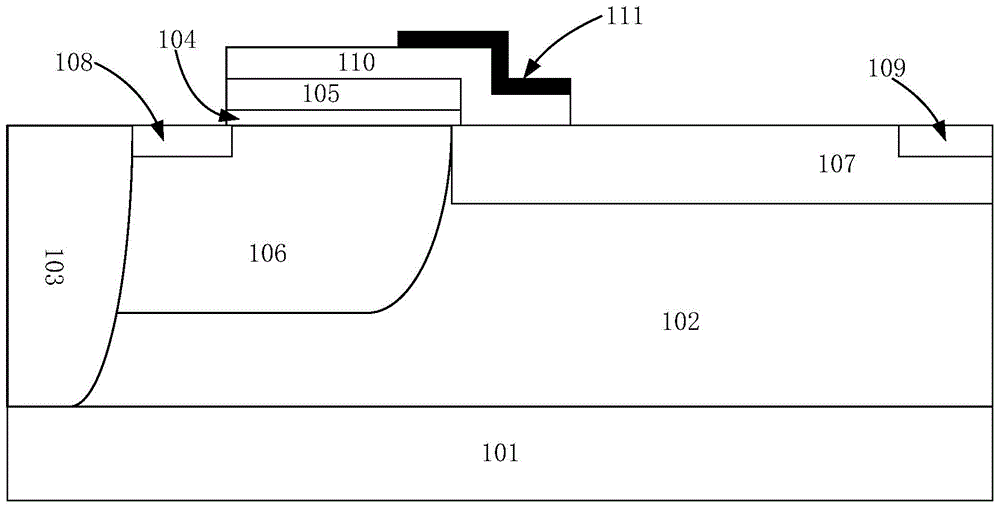
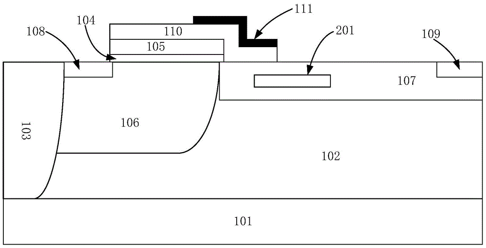
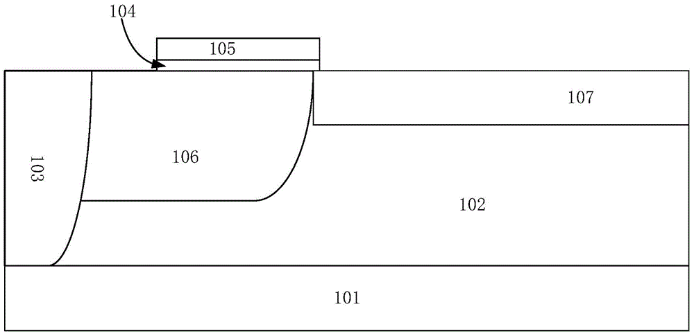
[0030] Such as figure 2 As shown, this example includes a P-type substrate 101 and a P-type epitaxial layer 102 located on the upper surface of the P-type substrate 101; the P-type epitaxial layer has P+sinker 103 and N-type lightly doped regions 107 on both sides, and the There is a P-type well region 106 between the P+sinker 103 and the N-type lightly doped region 107; the upper layer of the P-type well region 106 has a first N-type heavily doped region 108, and the first N-type heavily doped region 108 It is connected to the side of the P+sinker 103; the upper layer of the N-type lightly doped region 107 has a second N-type heavily doped region 109 on the side away from the P-type well region 106; the upper surface of the P-type well region 106 has a gate oxide Layer 104, the upper surface of the gate oxide layer 104 has a polysilicon gate 105, and the gate oxide layer 104 and the polysilicon gate 105 form a gate structure; the upper surface of the gate structure and the s...

Embodiment 2

[0046] Such as Image 6 As shown, on the basis of Embodiment 1, the oxide layer region 201 is changed into two regions of the oxide layer region 601 and the oxide layer region 602 located on the same horizontal plane, so as to achieve more flexible control of the influence of the oxide layer region on device performance . It can also be changed into multiple oxide layer regions on the same horizontal plane according to specific circumstances.

Embodiment 3

[0048] Such as Figure 7 As shown, on the basis of the first embodiment, this example has a device structure with double-layer field plates. The principle of this example is the same as that of Embodiment 1. The invention is also applicable to device structures having multilayer field plates.


PUM


Abstract

The invention relates to semiconductor technologies and especially relates to a radio frequency LDMOS device and a manufacturing method thereof. The method mainly comprises the following steps of introducing an oxide layer region into an N type light doped region on a device drain end; by adjusting the length, thickness and position of the oxide layer region, reducing the effective dielectric constant of a drift region on the premise that the device breakdown voltage and the conduction resistance are guaranteed to be not affected; thus reducing the device gate-drain capacitance and improving the device frequency characteristics. The technical scheme provided in the invention is especially suitably used for the LDMOS device and the manufacturing thereof.

Description

technical field [0001] The invention relates to semiconductor technology, in particular to a radio frequency LDMOS device and a manufacturing method thereof. Background technique [0002] RF LDMOS (Laterally Double-Diffused Metal Oxide Semiconductors, laterally double-diffused transistors) devices are a new generation of integrated solid-state microwave power semiconductor products that integrate semiconductor integrated circuit technology and microwave electronics technology. It maintains the advantages of ordinary MOSFETs. , the channel region is formed by lateral double diffusion technology, and a drift region is introduced between the drain and the channel. The radio frequency (RF) LDMOS device has high gain, high transconductance, good frequency response, high linearity, simple control, The advantages of fast switching speed, good thermal stability, and easy integration with CMOS circuits are widely used in mobile base stations and power integrated circuits. [0003] T...

Claims


Application Information

Patent Timeline
Patent Type & Authority Applications(China)
IPC IPC(8): H01L29/78H01L29/36H01L21/336
CPCH01L29/7816H01L29/36H01L29/66681
Inventor 邓小川甘志梁坤元张晓菲萧寒李妍月唐亚超张波
Owner UNIV OF ELECTRONICS SCI & TECH OF CHINA
Why Eureka
Try Eureka