

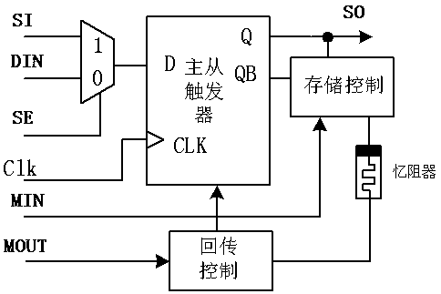
A scanning flip-flop circuit based on HP memristor and its design method
A technology of scanning triggers and memristors, applied in the direction of electric pulse generator circuits, etc., can solve the problems of damaged chips or test equipment, high power consumption, etc., and achieve the effect of reducing test power consumption
- Summary
- Abstract
- Description
- Claims
- Application Information
AI Technical Summary
Problems solved by technology
Method used
Image

Examples
Embodiment Construction
[0027] The technical solution of the present invention will be specifically described below in conjunction with the accompanying drawings.
[0028] The design process of the HP memristor-based scanning flip-flop circuit of the present invention is as follows,
[0029] Step S01: Using the existing CMOS master-slave flip-flop circuit technology; using the nano-scale memristive device announced by Hewlett-Packard in 2008, which has a power-off memory function, and its mathematical model is as follows:
[0030]
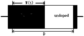
[0031]Among them, RMEM is the resistance value of the memristor, V(t) is the voltage across the memristor, w(t) represents the change of the width of the doped region with time, and D represents the total length of the doped region and the non-doped region , ROFF represents the resistance value of the memristor when the doped region is 0, RON represents the resistance value of the memristor when the non-doped region is 0, and the value of w(t) is automatically between ...
PUM
 Abstract
Description
Claims
Application Information