A kind of solar cell epitaxial wafer and its manufacturing method
A solar cell and manufacturing method technology, applied in the field of solar cells, can solve problems such as corrosion, production line yield drop, slow GaAs cell layer and substrate, etc., to reduce damage, reduce direct contact time, and reduce direct contact time Effect
- Summary
- Abstract
- Description
- Claims
- Application Information
AI Technical Summary
Problems solved by technology
Method used
Image
Examples
Embodiment 1
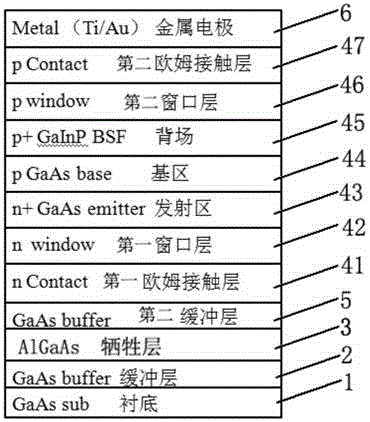
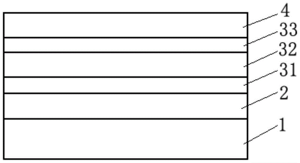
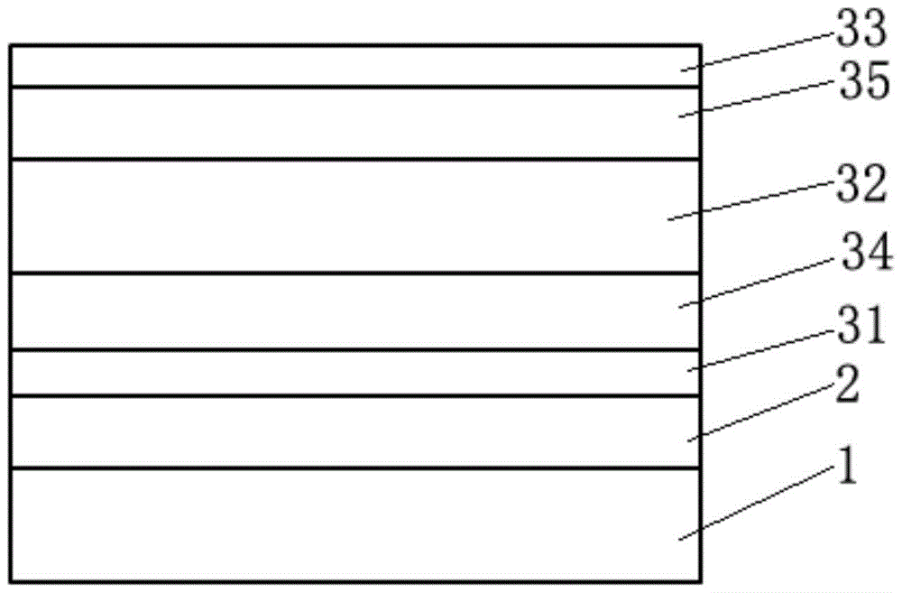
[0037] Such as figure 1As shown, this embodiment provides a solar cell epitaxial wafer, including a substrate 1, a buffer layer 2, a combined sacrificial layer 3 and a solar cell layer 4 arranged in sequence, and the combined sacrificial layer 3 includes a first sacrificial layer 31, a second The sacrificial layer 32 and the third sacrificial layer 33, the first sacrificial layer 31 is arranged close to the buffer layer 2, the third sacrificial layer 33 is arranged close to the solar cell layer 4, and the second sacrificial layer 32 is arranged between the first sacrificial layer 31 and the third sacrificial layer 31. Between the sacrificial layers 33 and the second sacrificial layer 32 are etched faster than the first sacrificial layer 31 and the third sacrificial layer 33 are etched.
[0038] For the solar cell epitaxial wafer provided in this embodiment, when the epitaxial lift-off process is performed, the part of the sacrificial layer away from the buffer layer 2 and the ...
Embodiment 2
[0050] Such as Figure 4 As shown, this embodiment provides a method for manufacturing a solar cell epitaxial wafer, for manufacturing the solar cell epitaxial wafer in the above-mentioned embodiment 1, comprising the following steps:
[0051] S1: growing the buffer layer 2 epitaxially on the substrate 1;
[0052] S2: Epitaxially grow a first sacrificial layer 31 on the buffer layer 2, and the first sacrificial layer 31 is close to the buffer layer 2;
[0053] S3: Epitaxially growing the second sacrificial layer 32 on the first sacrificial layer 31, the second sacrificial layer 32 is etched faster than the first sacrificial layer 31;
[0054] S4: epitaxially growing the third sacrificial layer 33 on the second sacrificial layer 32, the etching speed of the third sacrificial layer 33 is slower than that of the second sacrificial layer 32;
[0055] S5: epitaxially grow the solar cell layer 4 on the third sacrificial layer 33 to produce a solar cell epitaxial wafer, and the sol...
PUM
 Abstract
Description
Claims
Application Information


