Mechanical backdrilling method for PCB

A PCB board and back-drilling technology, applied in mechanical/acoustic circuit processing, electrical connection formation of printed components, electrical components, etc., to avoid the inability to protect the copper layer in the hole that should not be etched, enhance social competitiveness, and improve The effect of production efficiency

Inactive Publication Date: 2015-11-04
开平依利安达电子第五有限公司
View PDF4 Cites 13 Cited by
  • Summary
  • Abstract
  • Description
  • Claims
  • Application Information

AI Technical Summary

Problems solved by technology

[0010] In order to solve the technical problems existing in the existing VIA hole back-drilling design etching process, the purpose of the present invention is to provide a mechanical back-drilling method applied on a PCB, which protects the copper on the inner wall of the hole through the resin plug hole, so that the etching Remove the residual copper shavings after mechanical back drilling of VIA holes during the process, without affecting the hole copper in the resin protection part

Method used


Image

  • Mechanical backdrilling method for PCB
  • Mechanical backdrilling method for PCB
  • Mechanical backdrilling method for PCB

Examples


Embodiment Construction

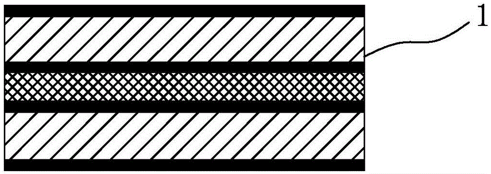
[0032] The present invention is mainly aimed at PCB multilayer circuit boards, and the mentioned mechanical back drilling method mainly processes VIA holes (diameter≤0.30mm).

[0033] refer to Figure 15 , the present invention provides a kind of mechanical back drilling method applied on PCB, comprising the following steps:

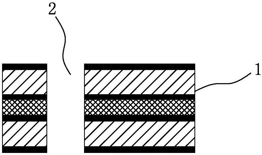
[0034] Z1: Drill a through hole 2 on the PCB board 1 with a superhard alloy drill bit. The diameter of the through hole 2 is preferably 0.30mm, such as Figure 10 shown;

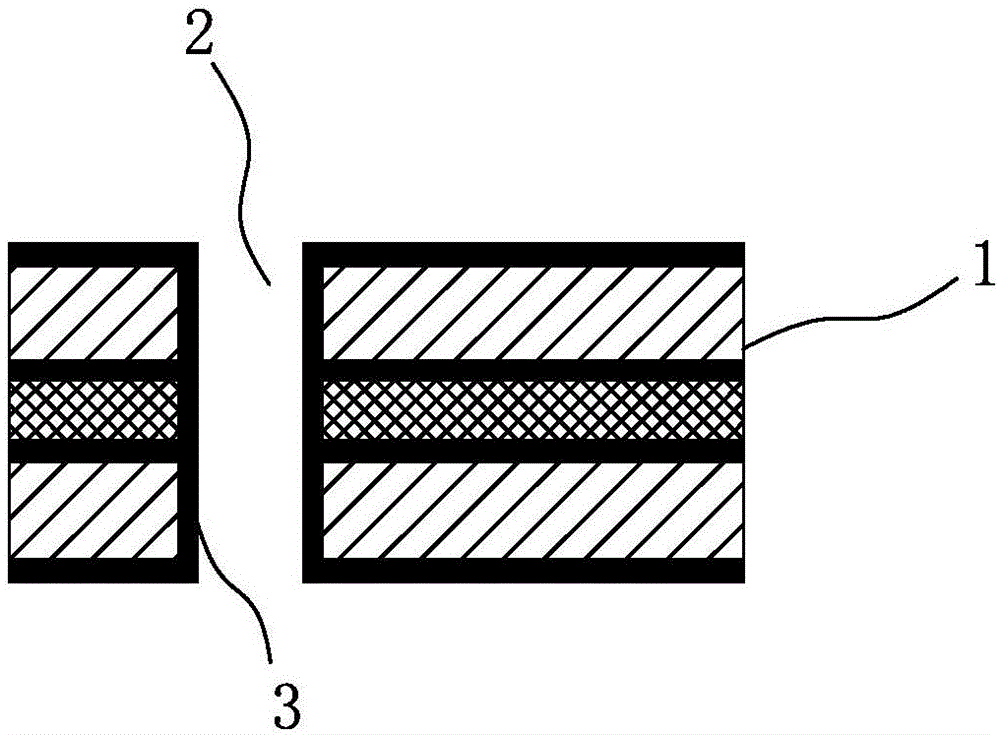
[0035] Z2: Copper layer 3 is electroplated on the inner wall of the through hole 2. The specific operation is as follows: the inner wall of the through hole 2 is made gold by electroless copper deposition, and then the copper layer 3 on the inner wall of the through hole 2 reaches the set value through the electroplating process. copper thickness, such as Figure 11 As shown, after this step is completed, the surface of the PCB 1 and the inner wall of the through hole 2 have been co...


PUM

PropertyMeasurementUnit
diameteraaaaaaaaaa

Abstract

The invention discloses a mechanical backdrilling method for a PCB. The method comprises the following steps that through holes are drilled in the PCB; the inner wall of the through hole is electro-plated with a copper layer; resin is filled into the through hole whose inner wall is covered with the copper layer; depth-controlled backdrilling is carried out on the through hole into which the resin is filled; and copper scarps in the backdrilling hole are removed by etching. The mechanical backdrilling method can protect the copper layer at the inner wall of the through hole by filling the resin into the hole, the part, protected by the resin, of the copper layer is not influenced in the etching process, secondary copper and tin plating are not needed, the problem that the diameter of the through hole is decreased caused by twice copper electroplating at the inner wall of the through hole is solved, and the phenomenon that an electroplated tin layer cannot protect the copper layer, which should not be etched, in the hole is avoided. Mechanical backdrilling is carried out after the resin is filled, so that the depth-controlled tolerance of the mechanical drilling hole is strictly controlled within the range of +/-0.075mm, the production efficiency is improved, and the social competitiveness of enterprise is improved.

Description

technical field [0001] The invention relates to a mechanical back drilling method applied on a PCB board. Background technique [0002] At present, with the continuous promotion of the information industry, the speed of digital signal transmission is getting faster and higher, the frequency is getting higher and higher, and the use of high-power amplifiers, the traditionally designed PCB board can no longer meet the requirements of this high-frequency circuit. need. In the design and production process of PCB circuit boards, back drilling is more and more widely used. For electronic products with high frequency circuits, back drilling is an important aspect of process requirements. [0003] In the manufacturing process of the PCB circuit board, the connection between the lines of each layer is realized through copper-plated through-holes. Some copper-plated through holes only need partial layer conduction to realize their functions, but after the PCB circuit board has unde...

Claims


Application Information

Patent Timeline
Patent Type & Authority Applications(China)
IPC IPC(8): H05K3/00
CPCH05K3/0047H05K3/42H05K2203/02
Inventor 张伟连
Owner 开平依利安达电子第五有限公司
Why Eureka
Try Eureka