Panel and testing method of same

A technology of panel and test pad, applied in the field of panel and its testing, can solve the problem of high testing complexity of touch electrode layer

Active Publication Date: 2015-11-11
HEFEI BOE OPTOELECTRONICS TECH +1
View PDF14 Cites 16 Cited by
  • Summary
  • Abstract
  • Description
  • Claims
  • Application Information

AI Technical Summary

Problems solved by technology

[0015] Embodiments of the present invention provide a panel and a testing method thereof, which are used to solve the problem of high testing complexity in the testing of the touch electrode layer in the prior art

Method used


Image

  • Panel and testing method of same
  • Panel and testing method of same
  • Panel and testing method of same

Examples


Embodiment Construction

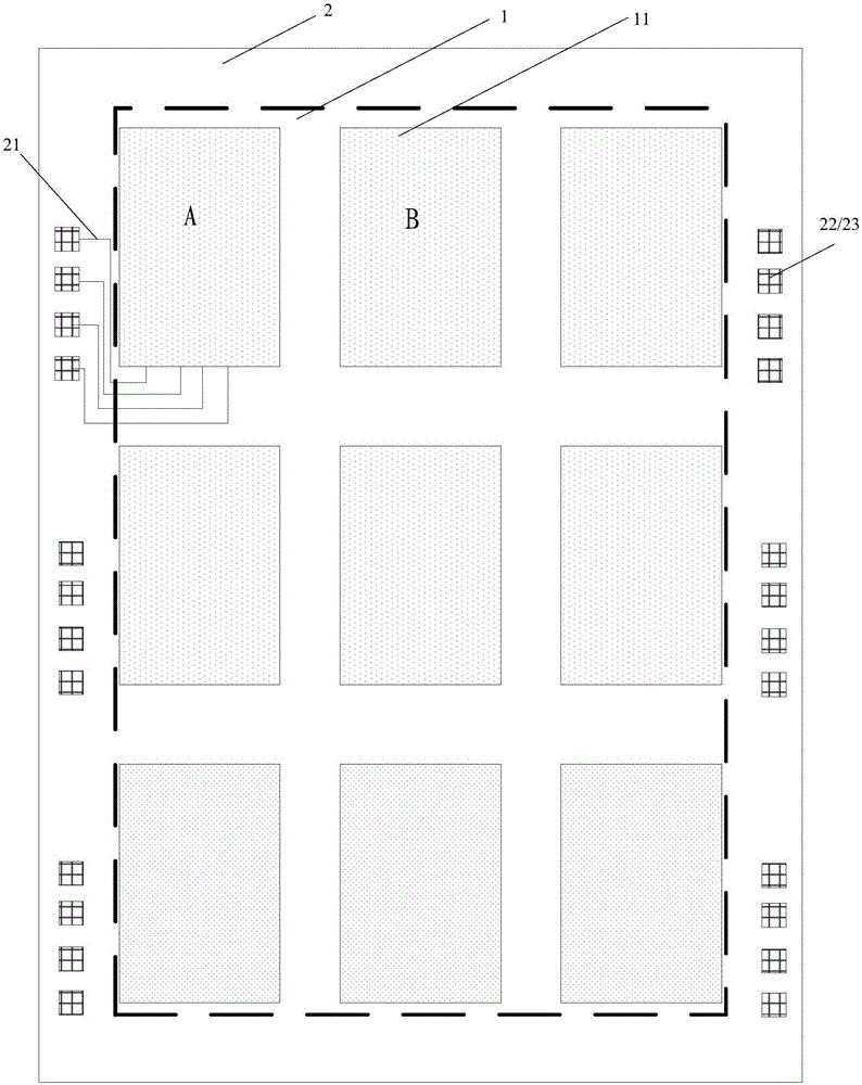
[0041] In order to solve the problem of high test complexity in the test of the touch electrode layer in the prior art, an embodiment of the present invention provides a panel and a test method thereof.
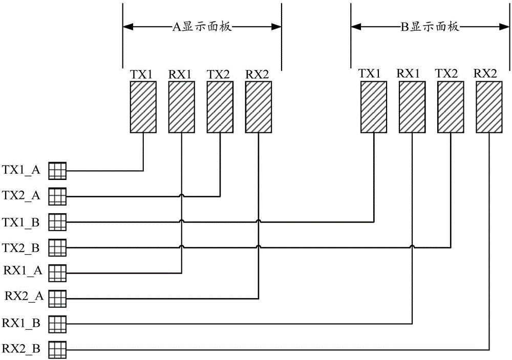
[0042] The main idea of ​​the embodiment of the present invention is to build a test environment on the panel (without cutting) with the touch electrode layer, and then conduct a test based on the test environment, and then cut it after the test to obtain a single display panel. In this test environment, the smaller drive signal input pin on the display panel is connected to the first test pad outside the display panel through the first test line, and the smaller inter-channel capacitance output pin on the display panel is connected to the display panel. The second test pad outside the panel is connected through the second test line, and the above connection needs to ensure that when the touch electrode layer is tested, for any channel pair, when connected to the first channel...


PUM


Abstract

The invention provides a panel and a testing method of the same in order to solve the problem in the prior art that testing of a touch-control electrode layer is very complicated. The panel comprises a plurality of display panels and testing wires as well as a first testing pad and a second testing pad, wherein the display panel comprises a drive signal input pin, an inter-channel capacitance output pin as well as touch-control electrode layers of a first channel and a second channel which are arranged alternately, the first channel is bound with the drive signal input pin, the second channel is bound with the inter-channel capacitance output pin, and the first channel and the adjacent second channel form a channel pair; the testing wire comprises a first testing wire which is used to connect the first testing pad and the drive signal input pin and a second testing wire which is used to connect the second testing pad and the inter-channel capacitance output pin; and aiming at each channel pair, a capacitance between the first channel and the second channel can be output from the second testing pad connected with the second channel when a drive signal is input into the first testing pad connected with the first channel of the same.

Description

technical field [0001] The invention relates to the technical field of manufacturing liquid crystal display devices, in particular to a panel and a testing method thereof. Background technique [0002] The integration of touch panel and liquid crystal panel includes "In-cell" method and "On-cell" method. Among them, OnCell refers to the method of embedding the touch screen between the color filter substrate and the polarizer of the display screen, that is, a touch sensor is equipped on the liquid crystal panel. The structure of a common oncecell is a glass substrate, a lower polarizer, a TFT (Thin Film Transistor, thin film transistor) substrate, a touch electrode layer, and an upper polarizer from bottom to top. The main process flow for forming this structure includes the following steps: [0003] The first step: After the TFT substrate and the color filter substrate are boxed together, a layer of ITO (Indium Tin Oxides, indium tin metal oxide) is deposited on the upper ...

Claims


Application Information

Patent Timeline
Patent Type & Authority Applications(China)
IPC IPC(8): G02F1/13G06F3/044
CPCG02F1/1309G06F3/044
Inventor 姜清华史高飞
Owner HEFEI BOE OPTOELECTRONICS TECH
Why Eureka
Try Eureka