Ceramic packages and electronic devices
A technology of ceramic packaging and ceramic substrate, which is applied in the direction of semiconductor devices, electric solid devices, semiconductor/solid device components, etc., can solve the problems of cracks in insulating substrates and increased thermal stress, and achieve crack suppression, yield improvement, gas The effect of high reliability
- Summary
- Abstract
- Description
- Claims
- Application Information
AI Technical Summary
Problems solved by technology
Method used
Image
Examples
Embodiment
[0067] [Ceramic substrate]
[0068] First, when carrying out the first to third examples described below, various types of ceramic substrates (substrates 1 to 17) constituting the container 12 are prepared.
[0069] (substrate 1)
[0070] The raw material powder is Al with an average particle size of 1.5 μm2 o 3 Powder, MgO powder with an average particle size of 0.5 μm, SiO with an average particle size of 4.0 μm 2 Powder, MnCO with an average particle size of 3.0 μm 3 Powder and TiO with an average particle size of 0.25 μm 2 powder.
[0071] Raw material powder by the ratio shown in following table 2 (Al 2 o 3 Powder: 91.0% by mass, MgO powder: 0.30% by mass, SiO 2 Powder: 4.0% by mass, MnCO 3 Powder: 4.7% by mass (2.9% by mass in terms of MnO), TiO 2 Powder: 1.0% by mass) were mixed to obtain a mixed powder. SiO 2 and MnCO 3 The content ratio (SiO 2 / MnCO 3 ) by SiO 2 / MnO conversion is 1.38. In the obtained mixed powder, polyvinyl butyral, tertiary amine, a...
no. 1 Embodiment
[0119] For Examples 1 to 12 and Comparative Examples 1 to 3, the same type of ceramic substrate was used, and the ratio of the additive (B or P) to the main component (Ni) of the stress relaxation layer was changed, and the change in film hardness at this time was confirmed. And the occurrence rate of cracks after hermetic sealing.
Embodiment 1
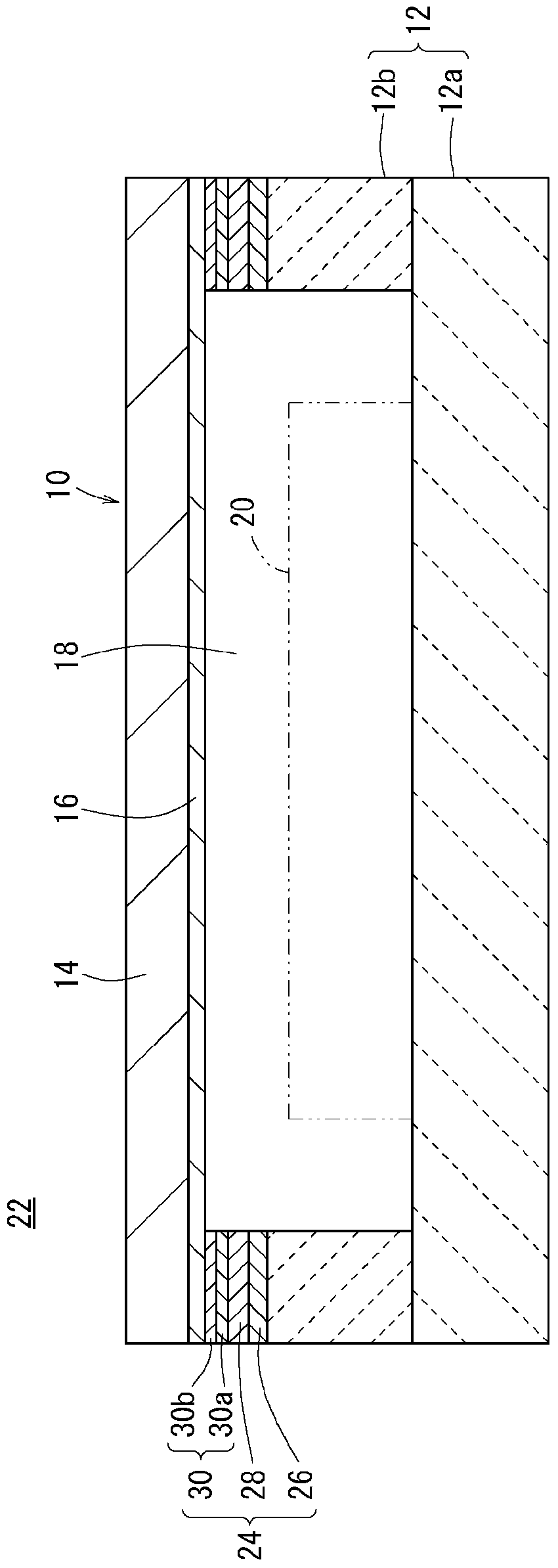
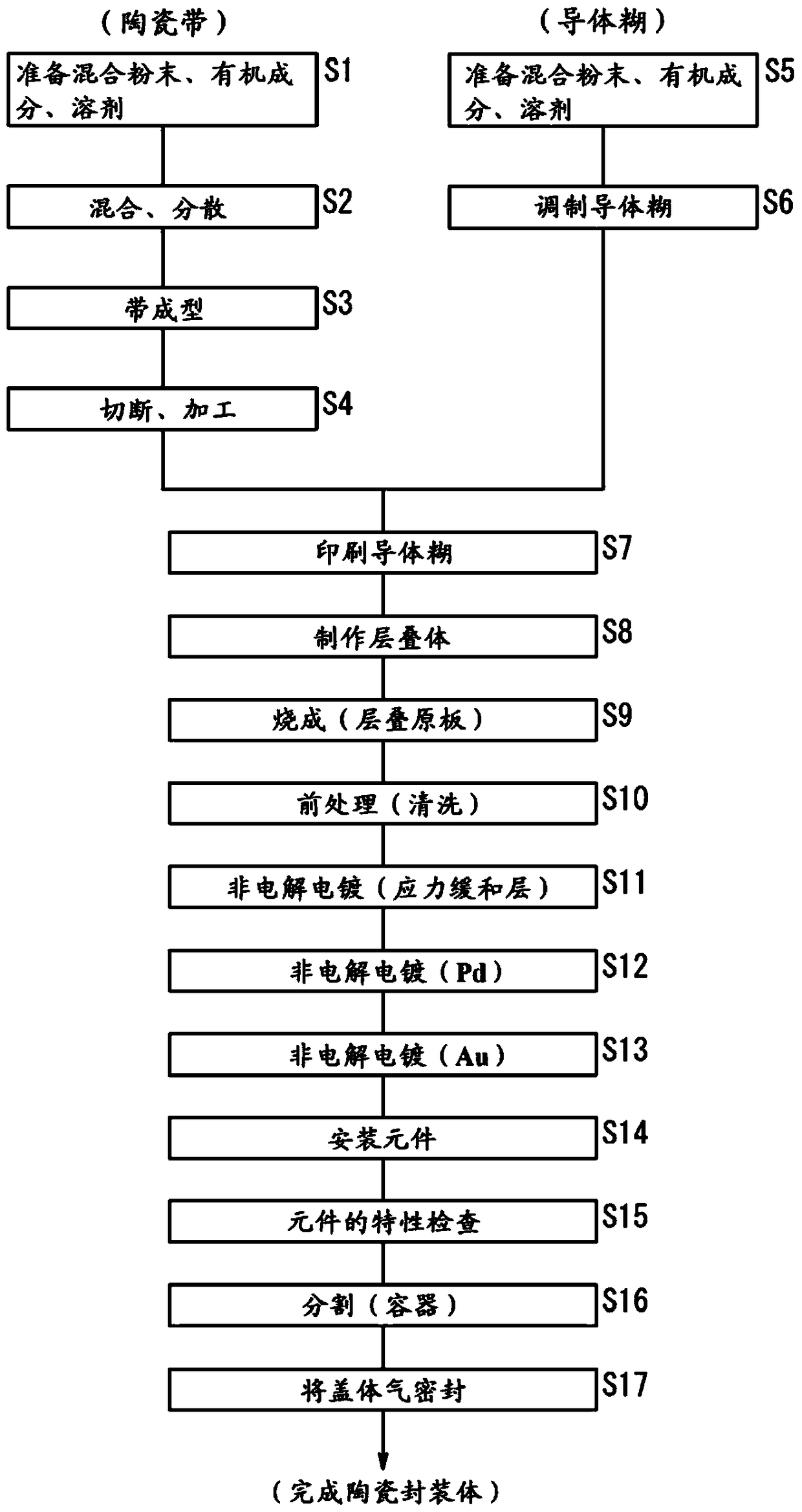
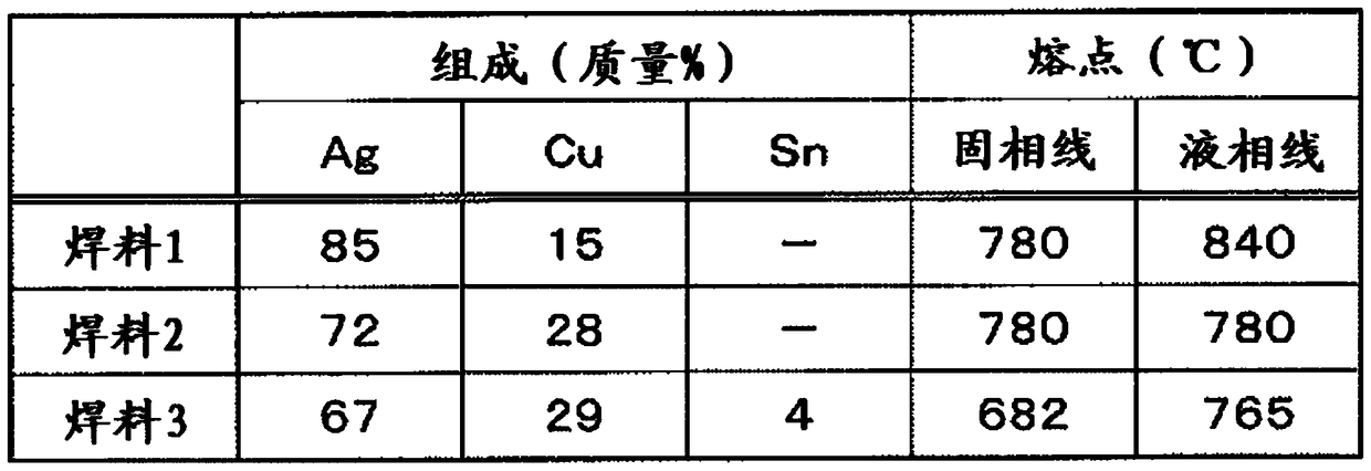
[0121] As the ceramic substrate, substrate 1 is used, as the conductor paste, paste 1 is used, and the composition of the stress relaxation layer 28 is Ni-B (B is 0.9% by mass), based on figure 2 With the manufacturing method shown, 625 samples 1 were produced. As the high-temperature sealing material 16, the brazing material 3 in Table 1 above was used. In addition, the film thickness of the stress relaxation layer 28 was set to 3 μm. Similarly, 625 samples 2 to 6 were prepared using pastes 2 to 6 as conductor pastes. Take this as Example 1.
PUM
| Property | Measurement | Unit |
|---|---|---|
| thickness | aaaaa | aaaaa |
| bending strength | aaaaa | aaaaa |
| thickness | aaaaa | aaaaa |
Abstract
Description
Claims
Application Information


