
A ceramic pin housing structure and manufacturing method thereof

A shell and ceramic technology, applied in semiconductor/solid-state device manufacturing, semiconductor/solid-state device components, semiconductor devices, etc., can solve problems such as inability to assemble and weld, air tightness problems, and inability to fill solder, so as to improve air tightness. The effect of reliability

Active Publication Date: 2020-07-24
NO 55 INST CHINA ELECTRONIC SCI & TECHNOLOGYGROUP CO LTD
View PDF7 Cites 0 Cited by
  • Summary
  • Abstract
  • Description
  • Claims
  • Application Information

AI Technical Summary

Problems solved by technology

If the gap is too narrow, the lead pins cannot be inserted smoothly, so that assembly and welding cannot be performed; if the gap is too wide, the solder cannot be filled, resulting in soldering holes
And a slight fluctuation in the size of the gap will also cause the amount of solder to be unable to be precisely controlled, resulting in airtightness problems

Method used


Image

  • A ceramic pin housing structure and manufacturing method thereof
  • A ceramic pin housing structure and manufacturing method thereof

Examples


Embodiment

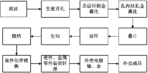
[0040] Manufacturing the ceramic pin shell structure includes the following steps:

[0041] 1) Using tape casting equipment at a drying temperature of 120°C to obtain a sheet of raw porcelain tape with a thickness of 0.34mm and a length and width of 210mm;

[0042] 2) Take 4 layers of 0.34 thick aluminum nitride raw porcelain tape, and use a mechanical punching machine to open the holes required for the lead pin;

[0043] 3) Use a printing machine and a screen screen to coat the top surface and the bottom surface with tungsten paste to obtain the metallized area required for the welding end seal of the ceramic part and the Kovar sealing ring and the metal required for welding with the Kovar frame chemical area, to dry;

[0044] 4) After drying, use the stencil screen and printing machine to open holes for the tungsten paste on the outermost layer of the porcelain tape to realize the metallization of the inner wall, and obtain the metallization area of ​​the guide pin and the ...


PUM

PropertyMeasurementUnit
thicknessaaaaaaaaaa
thicknessaaaaaaaaaa

Abstract

The invention relates to a shell structure and a manufacturing method of a ceramic pin. The shell structure is a combination of an end seal and a shaft seal between a ceramic part and a metal lead pin. The manufacturing method includes the following process steps: 1) Obtain alumina green porcelain tape by casting; 2) Open holes in each layer of alumina green porcelain tape; 3) Print the outermost layer and the bottommost layer of porcelain tape to obtain The metallization required for welding the ceramic parts and the shell frame; 4) Hanging holes are made on the outermost layer of the porcelain tape; 5) Obtaining a single cooked porcelain piece; 6) Electroless nickel plating is used; 7) The semi-finished shell is made; 8) Made into a finished package enclosure. Advantages: It can effectively improve the airtight reliability of high-reliability power electronic packaging shells, and can ensure the batch preparation of this type of products for large-scale production processes.

Description

technical field [0001] The invention relates to a ceramic pin housing structure and a manufacturing method thereof, which is aimed at the structure and manufacturing method of a packaging housing for power electronics, and belongs to the technical field of ceramic packaging. Background technique [0002] Ceramic pin housings are widely used in high-reliability packaging of power electronic devices, such as typical To254 and To256 series packaging. There are generally two types of sealing forms for the pins of this type of packaging shell, one is end sealing and the other is shaft sealing. Both sealing forms have a certain proportion of airtightness problems in the production process. [0003] For the end seal structure, the surface bonding is formed by welding the surface of the welding ring and the porcelain part, and the gap between the lead pin and the welding ring is filled with silver-copper solder to form a sealing structure of the welding ring, porcelain part and lead...

Claims


Application Information

Patent Timeline
Patent Type & Authority Patents(China)
IPC IPC(8): H01L23/04H01L23/08H01L21/48
CPCH01L21/4803H01L21/4807H01L23/04H01L23/08
Inventor 陈寰贝陈宇宁周昊
Owner NO 55 INST CHINA ELECTRONIC SCI & TECHNOLOGYGROUP CO LTD
Learn More