Test method for residual stress of subsurface of grinding wafer

A technology of residual stress and testing method, which is applied in the direction of measurement, measuring device, instrument, etc. by measuring the change force of the optical properties of the material when it is stressed, to achieve the effect of ensuring accuracy and simple principle

Inactive Publication Date: 2015-11-18
BEIJING UNIV OF TECH
View PDF6 Cites 5 Cited by
  • Summary
  • Abstract
  • Description
  • Claims
  • Application Information

AI Technical Summary

Problems solved by technology

The experimental method mainly solves the corrosion depth test and the residual stress test of the ground wafer subsurface, and the data processing method mainly solves the corrosion depth calculation and residual stress calculation problems

Method used


Image

  • Test method for residual stress of subsurface of grinding wafer
  • Test method for residual stress of subsurface of grinding wafer
  • Test method for residual stress of subsurface of grinding wafer

Examples


Embodiment Construction

[0023] The test method that the present invention proposes comprises the following steps:

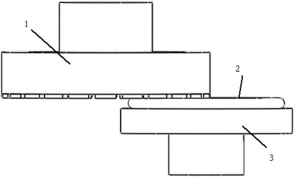
[0024] 1: Grinding wafers: adjust the grinding parameters of the grinding machine, select the wafers to be ground, transfer the wafers to the grinding station, absorb the wafers with the suction cup, and grind the wafers.

[0025] 2: Wafer cleaning: The wafer is transferred to the cleaning table by the robot, and the surface of the wafer is rinsed to remove residual abrasive debris.

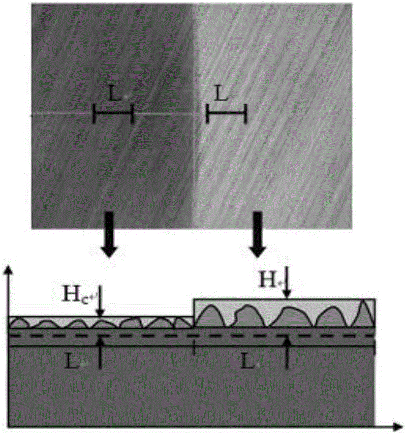
[0026] 3: Fix the wafer on the fixture, clean the wafer with an organic solvent for the second time, determine the test position, and use "Young's" solution to corrode each test point. Each test point is corroded 8 times in total, and the time for each corrosion is 2s, 3s, 4s, 5s, 10s, 15s, 25s, 40s respectively, and then clean the corrosion position to terminate the corrosion process.

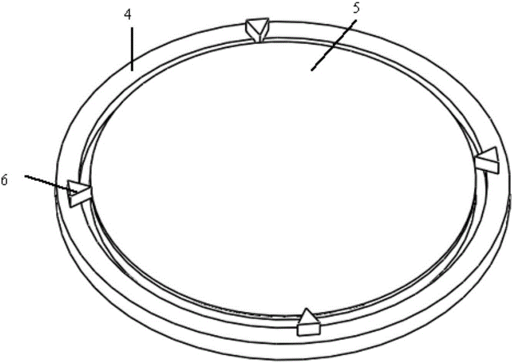
[0027] 4: Fix the wafer on the stage of the white light interferometer to test the corrosion depth; use Raman spectrosc...


PUM

PropertyMeasurementUnit
thicknessaaaaaaaaaa
thicknessaaaaaaaaaa

Abstract

The invention provides a test method for the residual stress of a subsurface of a grinding wafer, and belongs to the field of tests of the residual stress. The method includes steps: providing the grinding wafer; cleaning the wafer via high-pressure water; fixing the wafer; determining the corrosion position, and performing corrosion and cleaning; testing the corrosion depth and the residual stress by respectively employing a white light interferometer and a laser Raman spectroscopy; and repeating the above experiment steps to obtain the residual stress value of the subsurface of the grinding wafer. According to the method, the operation is simple, the residual stress for grinding the subsurface of the wafer can be accurately obtained, and an optimized scheme of the grinding process can be proposed via the analysis of test results.

Description

technical field [0001] The invention relates to a method for testing the subsurface residual stress of a grinding wafer, in particular to a method for testing the subsurface residual stress of a grinding wafer by distributed corrosion and Raman spectroscopy. Background technique [0002] With the rapid development of IC manufacturing technology, in order to increase the output of IC chips and reduce the cost of unit manufacturing, the diameter of wafers tends to be larger, and the size of wafers has grown from the initial 2 inches to the currently widely used 8 inches, and even to larger sizes. direction development. As the diameter of the wafer increases, in order to ensure that the wafer has sufficient strength, the thickness of the wafer also increases accordingly. At present, the average thickness of 8-inch wafers is 725 microns, while the average thickness of 12-inch wafers has increased to 775 microns. On the contrary, in order to meet the needs of IC chip packaging, ...

Claims


Application Information

Patent Timeline
Patent Type & Authority Applications(China)
IPC IPC(8): G01L1/24G01B11/22
Inventor 秦飞孙敬龙安彤陈沛宇慧平王仲康唐亮
Owner BEIJING UNIV OF TECH
Why Eureka
Try Eureka