Anti-shock surge circuit applied to ruggedized computer
A technology for strengthening computers and surge circuits, applied in the direction of data processing power supply, etc., can solve problems such as power supply failures, and achieve the effect of simple circuit, high reliability, and guaranteed reliability.
- Summary
- Abstract
- Description
- Claims
- Application Information
AI Technical Summary
Problems solved by technology
Method used
Image
Examples
Embodiment 1
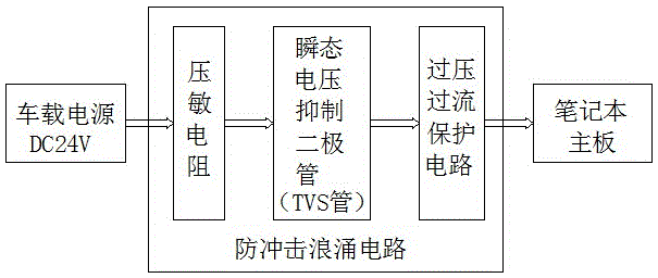
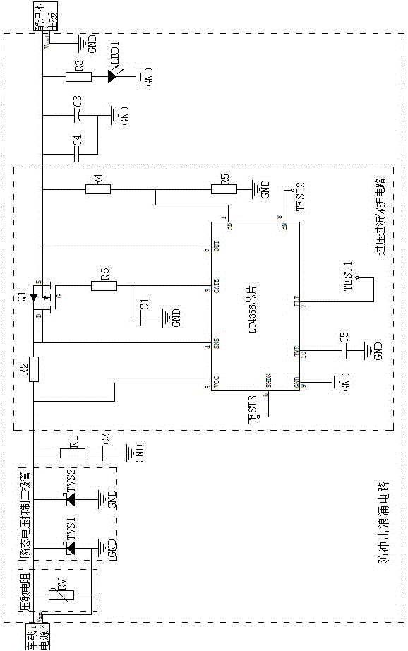
[0029] An anti-shock and surge circuit applied to a reinforced computer of the present invention, its structure includes a power supply input terminal Vin, a varistor RV, a transient voltage suppression diode TVS, an overvoltage and overcurrent protection circuit, and a power supply output terminal connected in sequence Vout; the varistor RV, the transient voltage suppression diode TVS, and the overvoltage and overcurrent protection circuit are connected in parallel. The other end of the suppression diode TVS is grounded; the overvoltage and overcurrent protection circuit includes an overvoltage protection regulator chip and a linear field effect transistor Q1. The VCC pin of the overvoltage protection regulator chip is connected to the power input terminal Vin, and the overvoltage protection regulator The OUT pin of the chip is connected to the power supply output terminal Vout; the drain (D) of the linear field effect transistor Q1 is connected to the SNS pin of the overvolta...
Embodiment 2
[0048] An anti-shock and surge circuit applied to a reinforced computer of the present invention, its structure includes a power supply input terminal Vin, a varistor RV, a transient voltage suppression diode TVS, an overvoltage and overcurrent protection circuit, and a power supply output terminal connected in sequence Vout; the varistor RV, the transient voltage suppression diode TVS, and the overvoltage and overcurrent protection circuit are connected in parallel. The other end of the suppression diode TVS is grounded; the overvoltage and overcurrent protection circuit includes an overvoltage protection regulator chip and a linear field effect transistor Q1. The VCC pin of the overvoltage protection regulator chip is connected to the power input terminal Vin, and the overvoltage protection regulator The OUT pin of the chip is connected to the power supply output terminal Vout; the drain (D) of the linear field effect transistor Q1 is connected to the SNS pin of the overvolta...
PUM
 Abstract
Description
Claims
Application Information

