Device structure with grapheme as contact electrode and manufacturing method thereof

A graphene electrode and device structure technology, applied in the field of microelectronics, can solve the problems of electrode contact resistance affecting device performance, lattice damage, material surface pollution, etc.

Active Publication Date: 2015-11-18
SHANGHAI INST OF MICROSYSTEM & INFORMATION TECH CHINESE ACAD OF SCI
View PDF4 Cites 16 Cited by
  • Summary
  • Abstract
  • Description
  • Claims
  • Application Information

AI Technical Summary

Problems solved by technology

In addition, the existing device preparation processes such as wet transfer, photolithography, etching, metal deposition and other processes will cause material surface contamination, wrinkles and lattice damage, etc. In addition, too large electrode contact resistance will seriously affect device performance.

Method used


Image

  • Device structure with grapheme as contact electrode and manufacturing method thereof
  • Device structure with grapheme as contact electrode and manufacturing method thereof
  • Device structure with grapheme as contact electrode and manufacturing method thereof

Examples


Embodiment 1

[0047] Please refer to the attached Figure 1-16 As shown, the present invention provides a kind of device structure preparation method using graphene as contact electrode, and the specific implementation method is as follows:

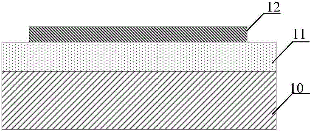
[0048] Step 1, forming a polypropylene carbonate PPC film 11 on the first substrate 10; PPC is coated on the first substrate 10 at 1500r / min with a glue leveler, and heated at 120 degrees for 3-5min until it is cured to form a film; then a mechanically peeled first h-BN film 12 is formed on the PPC film. A PPC-h-BN structure on the first substrate is formed. see figure 1 shown.

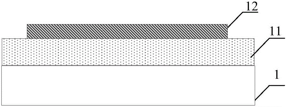
[0049] In step 2, peel off the PPC-h-BN structure on the first substrate 10 and place it on the PDMS film 1 to form a PDMS-PPC-h-BN structure. The surface of the PDMS film 1 and the PPC film is smooth and elastic. Since the PDMS film is relatively thick, it plays a supporting role in the subsequent dry transfer process and can be well adhered to the PPC film by van der Wa...

Embodiment 2

[0065] The present invention also provides another device structure preparation method using graphene as a contact electrode, which at least includes the steps:

[0066] a) see Figure 17 As shown, a polypropylene carbonate PPC film 11' is formed on the first substrate 10'; PPC is coated on the first substrate 10' at 1500r / min with a glue leveler, and heated at 120 degrees for 3 -5min until solidified into a film; then form a mechanically peeled h-BN film 12' on the PPC film 11';

[0067] b) Peel off the PPC-h-BN on the first substrate 10', and put it on the PDMS elastic film 1' with support and adhesion, please refer to the attached Figure 18 shown.

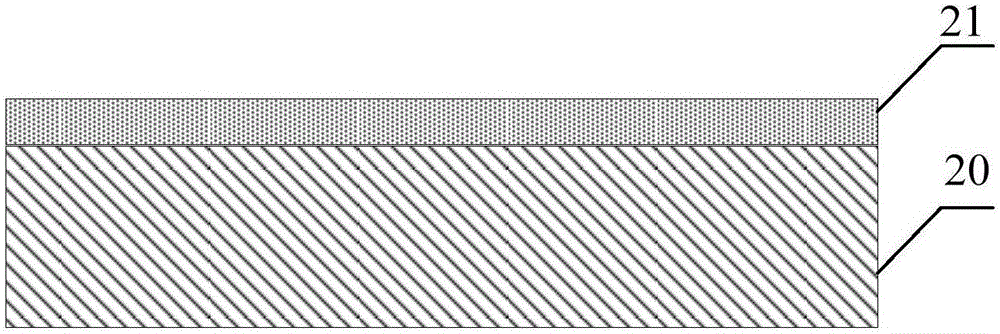
[0068] c) MoS is formed on the second substrate 30' 2 Film 31'; see Figure 19 shown.

[0069] d) Adsorption of MoS in step c) with the PDMS-PPC-h-BN structure 2 thin film; obtain PDMS—PPC—h-BN—MoS 2 structure; see Figure 20 and Figure 21 shown.

[0070] e) see Figure 22 and 23 As shown, a graphene film 21' is fo...


PUM


Abstract

The invention provides a device structure with grapheme as a contact electrode and a manufacturing method thereof, and relates to the technical field of device structures with grapheme as contact electrodes. A novel device structure of an h-BN-grapheme-superconductive / semi conducting material-h-Bh is formed through a dry transfer method, and pollution and damage of material crystal lattices due to wet transferring method, graphical etching and metallic deposition technology. h-BN services as a substrate and an encapsulated layer, which facilitates grapheme carrier mobility, and protects the device from absorbing O2, H2O and particles in air. The electric performance of the device structure is improved. The grapheme serves as contact electrode, and one-dimensional linear contact between the depositing metal and the cross section of the grapheme is formed. The contact resistance of superconductive / semiconductor devices is substantially reduced.

Description

technical field [0001] The invention belongs to the field of microelectronics, and relates to a device structure using graphene as a contact electrode and a preparation method thereof. Background technique [0002] Graphene, as the first discovered two-dimensional atomic crystal that can exist stably at room temperature, has been widely researched and applied in fields such as radio frequency transistors, logic switches, memories, sensors, and transparent conductive electrodes due to its excellent electrical properties. [0003] The birth of graphene has opened up people's extensive attention and exploration in the field of new two-dimensional electronic materials. Therefore, following graphene, researchers have discovered a series of two-dimensional semiconductor / superconducting materials with a single-layer atomic thickness, such as black scale, MoS 2 , MoSe, MoTe 2 、WSe 2 , WTe, TiSe 2 , PtSe 2 , PdSe 2 , CdS, CdSe, etc. These two-dimensional crystals can be used to...

Claims


Application Information

Patent Timeline
Patent Type & Authority Applications(China)
IPC IPC(8): H01B1/04H01G9/042H01L39/12H01L39/24H01L21/28
Inventor 王浩敏谢红李蕾王慧山贺立陈令修张道礼邓联文谢晓明江绵恒
Owner SHANGHAI INST OF MICROSYSTEM & INFORMATION TECH CHINESE ACAD OF SCI
Why Eureka
Try Eureka