Supercharge Your Innovation With Domain-Expert AI Agents!

Electroless plating method and ceramic substrate

A ceramic substrate, non-electrolytic technology, applied in printed circuits, electrical components, liquid chemical plating, etc., can solve problems such as plating thickness fluctuations, and achieve the effect of improving module reliability

Active Publication Date: 2015-11-18
MITSUBISHI ELECTRIC CORP
View PDF4 Cites 0 Cited by
  • Summary
  • Abstract
  • Description
  • Claims
  • Application Information

AI Technical Summary

Problems solved by technology

If the glass floats, there may be a non-plating state where nickel plating is not formed on the glass component, or the thickness of the plating may fluctuate

Method used


Image

  • Electroless plating method and ceramic substrate
  • Electroless plating method and ceramic substrate
  • Electroless plating method and ceramic substrate

Examples


Embodiment approach 1

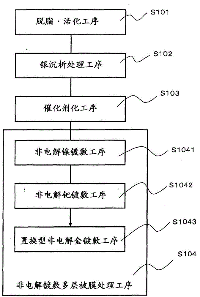
[0033] figure 1 It is a figure which shows the process flow of Embodiment 1 of this invention. figure 1 Among them, in terms of the electroless plating method in the glass-ceramic wiring board, it is the following method: the step of degreasing and activating the surface of the silver sintered body wiring pattern (step S101), the catalytic step (step S103), Electroless nickel plating process (step S1041), electroless palladium plating process (step S1042), and displacement type electroless gold plating process (step S1043), silver precipitation is carried out between the degreasing and activation process and the catalytic process. analysis process (step S102).

[0034] The electroless nickel plating process (step S1041), the electroless palladium plating process (step S1042), and the displacement type electroless gold plating process (step S1043) are collected as the electroless plating multilayer film treatment process (step S104).

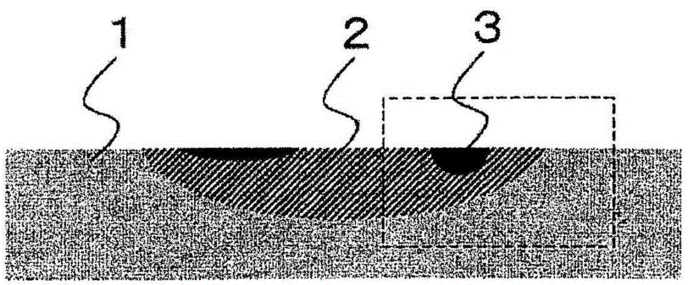
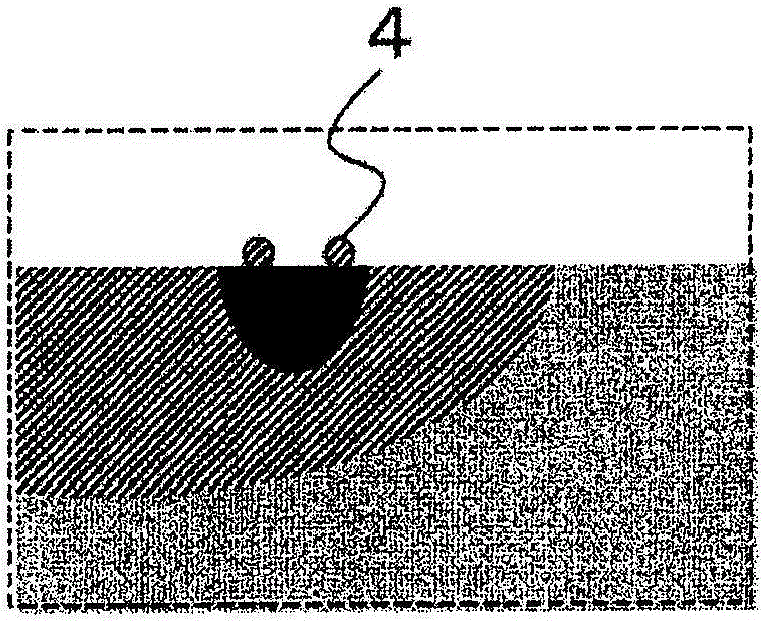
[0035] figure 2 It is a sectional vie...

Embodiment approach 2

[0079] Figure 9 It is a figure which shows the process flow of Embodiment 2 of this invention. In the previous Embodiment 1, the degreasing and activation process, the silver precipitation treatment process, the catalystization process, the electroless nickel plating process, the electroless palladium plating process, and the displacement type electroless gold plating process were performed in the order of The method of electrolytic plating is described. On the other hand, in Embodiment 2, in addition to Embodiment 1 above, a case where a glass etching step is performed between the electroless nickel plating step and the electroless palladium plating step will be described.

[0080] Between the silver sintered body wiring patterns 2 of Embodiment 1 above, if the pattern interval is narrow, for example, within 10 μm, palladium may be abnormally deposited on the deposited silver in the electroless palladium plating process, resulting in a pattern. short circuit between. Ther...

Embodiment approach 3

[0106] Figure 10 It is a figure which shows the process flow of Embodiment 3 of this invention. The method of performing electroless plating in the order of the electroless nickel plating step, the electroless palladium plating step, and the displacement type electroless gold plating step in the electroless plating multilayer film treatment step in the first embodiment Be explained. On the other hand, in Embodiment 3, the electroless plating multilayer film treatment step is performed in the order of electroless nickel plating step, displacement type electroless gold plating step, and reduction type electroless gold plating step. The method of plating will be described. Other configurations are the same as those in the first embodiment.

[0107] Figure 10 Among them, step S301, step S302, and step S303 are sequentially the same as those of the previous embodiment 1 figure 1 Step S101, step S102, and step S103 are the same process.

[0108] Next, step S304 of the electr...


PUM

PropertyMeasurementUnit
Particle sizeaaaaaaaaaa
The average particle sizeaaaaaaaaaa
Widthaaaaaaaaaa

Abstract

Provided is an electroless plating method comprising: a degreasing / activation treatment step in which the surface of a wiring pattern that comprises sintered silver and that is on a ceramic substrate is degreased and activated; a catalyzing step in which a catalyst is applied to the surface of the wiring pattern comprising sintered silver; and an electroless plating multilayer film treatment step in which an electroless plated film having multiple layers is formed on the surface of the wiring pattern comprising sintered silver. In addition, a silver precipitation treatment step in which silver is precipitated on a glass component that is present on the surface of the wiring pattern comprising sintered silver after the degreasing / activation treatment step is provided between the degreasing / activation treatment step and the catalyzing step, and at the catalyzing step, the catalyst is also applied to the silver precipitated at the silver precipitation treatment step.

Description

technical field [0001] The present invention relates to a ceramic substrate used as an electronic component package and a wiring substrate, and particularly to an electroless plating method for forming a plating film on the surface of a wiring pattern of an LTCC substrate, and to a ceramic substrate. Background technique [0002] Conventionally, ceramic substrates have been frequently used as wiring boards for packaging multi-chip modules on which passive components such as a plurality of semiconductor elements, capacitors, and resistors are mounted. As the ceramic substrate, a low-temperature-fired glass-ceramic substrate (LTCC substrate) or the like fired at a low temperature is used. In this case, the low temperature of the low-temperature fired glass ceramic substrate means a temperature range of 850°C to 1000°C. This LTCC substrate is composed of an insulating base material made of glass ceramics and a wiring pattern made of a sintered body mainly composed of a metal m...

Claims


Application Information

Patent Timeline
IPC IPC(8): C23C18/18
CPCC23C18/1844C23C18/1651C23C18/18C23C18/54C23C18/1639C23C18/44Y10T428/24917C23C18/1886C23C18/36H05K1/0306H05K1/092H05K3/185
Inventor 竹本洋平关野士郎改发雄太山中广美
Owner MITSUBISHI ELECTRIC CORP
Features
  • R&D
  • Intellectual Property
  • Life Sciences
  • Materials
  • Tech Scout
  • Unparalleled Data Quality
  • Higher Quality Content
  • 60% Fewer Hallucinations
Learn More