A Method for Induced Intermetallic Growth of Thin Films with Specific Grain Orientation and Quantity Using Laser Forward Transfer

A technology of intermetallic compounds and grain orientation, applied in chemical instruments and methods, metal layered products, metal processing equipment, etc., can solve the problems of high manufacturing cost, device damage, long time, etc. in tens of minutes or even hours. problems, to achieve the effect of improving thermal conductivity and mechanical properties, optimizing and improving microstructure, and improving high temperature service ability

Active Publication Date: 2017-02-22
HARBIN INST OF TECH
View PDF9 Cites 0 Cited by
  • Summary
  • Abstract
  • Description
  • Claims
  • Application Information

AI Technical Summary

Problems solved by technology

According to the thermodynamic properties of nano-silver particles, the connection can be realized under the condition of less than 200 ° C, and the formation of joints can be used under the condition of more than 350 ° C, but the connection of nanoparticles takes a long time, the joint is porous structure, and the preparation cost of nano-materials is relatively high. Higher, which restricts the application of such materials; joints formed by all-intermetallic compounds can be applied under high temperature conditions, but generally the preparation time is longer, tens of minutes or even hours, and the microstructure is difficult to control, so it is difficult to realize Large-scale industrial application; the sintering of intermetallic compound nanoparticles solder paste needs to be sintered with a specification higher than or close to the melting point of intermetallic compounds, and the melting point of intermetallic compounds is generally higher (over 400 ° C), which is easy to cause damage to the device during the connection process. damage

Method used


Image

  • A Method for Induced Intermetallic Growth of Thin Films with Specific Grain Orientation and Quantity Using Laser Forward Transfer
  • A Method for Induced Intermetallic Growth of Thin Films with Specific Grain Orientation and Quantity Using Laser Forward Transfer
  • A Method for Induced Intermetallic Growth of Thin Films with Specific Grain Orientation and Quantity Using Laser Forward Transfer

Examples


Embodiment 1

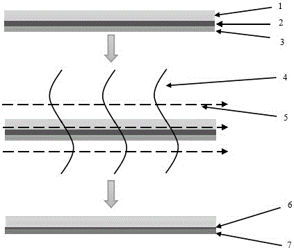
[0024] Such as Figure 1-3 As shown, the laser forward transfer Cu 3 Sn Single Crystal Thin Film Induced Preparation of Single Cu 3 The Sn interconnect solder joint method comprises the following steps:

[0025] Step 1: Prepare a Cu thin film as a seed layer on the surface of a transparent quartz substrate by magnetron sputtering, and the thickness of the seed layer is 50 nm.

[0026] Step 2: continue to prepare a Cu thin film with a thickness of 500 nm by electroplating.

[0027] Step 3: preparing a Sn film with a thickness of 400 nm on the surface of the Cu film by electroplating.

[0028] Step 4: Heating with a hot plate placed under the glass substrate for directional heating of the Cu / Sn double-layer film. The temperature of the hot plate is set at 360° C., the heating time is 200 h, and the heating environment is in a nitrogen environment. The direction of the applied magnetic field is parallel to the glass substrate. After heating, single crystal Cu 3 Sn.

[0029...

Embodiment 2

[0033] Such as Figure 1-3 As shown, the laser forward transfer Ag 3 Single Ag Induced by Sn Thin Film 3The Sn interconnect solder joint method comprises the following steps:

[0034] Step 1: Prepare an Ag thin film on the surface of the quartz substrate by evaporation, with a thickness of 300 nm.

[0035] Step 2: preparing a Sn film with a thickness of 100 nm on the surface of the Ag film by vapor deposition or other methods.

[0036] Step 3: heating the above-mentioned Ag / Sn double-layer film through a constant temperature furnace, the furnace temperature is set to 400° C., the heating time is 300 h, and the heating environment is in a nitrogen environment. Applied electric field, its direction is perpendicular to the quartz substrate. After heating, a single crystal of Ag is formed 3 Sn.

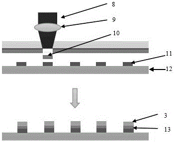
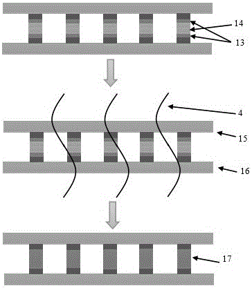
[0037] Step 4: using laser forward transfer technology to transfer the intermetallic compound film to the surface of the chip and the pad of the substrate respectively, the metal on...

Embodiment 3

[0041] Such as Figure 1-3 As shown, laser forward transfer Ni 3 sn 4 Thin film induced single Ni 3 sn 4 The method of interconnecting solder joints includes the following steps:

[0042] Step 1: preparing a Ni thin film on the surface of the quartz substrate by evaporation, with a thickness of 400 nm.

[0043] Step 2: preparing a Sn film with a thickness of 250 nm on the surface of the Ni metal film by vapor deposition or other methods.

[0044] Step 3: heating the above-mentioned Ni / Sn double-layer film through a constant temperature furnace, the temperature of the furnace is set at 350° C., the heating time is 500 h, and the heating environment is nitrogen environment. The direction of the applied magnetic field is perpendicular to the quartz substrate. Single crystal Ni formed after heating 3 sn 4 .

[0045] Step 4: Use laser forward transfer technology to transfer the intermetallic compound thin film to the surface of the chip and the substrate pad respectively. ...


PUM

PropertyMeasurementUnit
thicknessaaaaaaaaaa
thicknessaaaaaaaaaa
radiusaaaaaaaaaa

Abstract

The invention discloses a method for inducing growth of an intermetallic compound with the specific grain orientation and the specific number of films through laser forward transfer printing. The method comprises the following steps that firstly, a seed layer is prepared on the surface of a substrate; secondly, a metal film is continuously prepared on the surface of the seed layer; thirdly, the Sn film is prepared on the surface of metal film; fourthly, the substrate and the two films are heated, so that the intermetallic compound film is prepared; fifthly, the intermetallic compound film is transferred to the surfaces of a chip and bonding pads of the substrate respectively; sixthly, the surface of the intermetallic compound film is plated with the Sn film; and seventhly, the bonding pads are in butt joint, pressure is applied, the bonding pads are placed in a reflow furnace, and the stages of preheating, heat preservation, reflowing and cooling are performed. By the adoption of the method, the preparation time of a welding spot of the intermetallic compound capable of being used for high-temperature packaging and interconnection is greatly shortened, the grain orientation and the number of following growing intermetallic compounds are controlled, the welding spot of the intermetallic compound is quickly prepared, and the microstructure is controllable.

Description

technical field [0001] The invention belongs to the technical field of micro-interconnection of electronic packaging, and relates to a method for rapidly preparing intermetallic compound solder joints that can be used for high-temperature packaging and interconnection, and in particular to a method of using laser forward transfer printing with specific grain orientation and quantity film induction Methods of growth of intermetallic compounds. Background technique [0002] Electronic packaging micro-interconnection technology is one of the core technologies for packaging various electronic components and components. With the development of electronic components and components in the direction of high power and high density, the service temperature and working environment of electronic components and components become more severe, which will put forward higher requirements for the bonding materials of electronic components and components, However, traditional solder alloys an...

Claims


Application Information

Patent Timeline
Patent Type & Authority Patents(China)
IPC IPC(8): B23K1/19B23K1/20B32B15/00B32B17/06B32B38/00C23C14/16C23C14/18C23C14/58
CPCB23K1/19B23K1/20B32B15/00B32B17/061B32B38/00C23C14/16C23C14/18C23C14/5886
Inventor 刘威王春青田艳红安荣郑振
Owner HARBIN INST OF TECH
Why Eureka
Try Eureka