Method for detecting imaging position error of laser direct imaging equipment

A technology of laser direct imaging and error detection, which is applied in the direction of microlithography exposure equipment, photolithography exposure device, etc., can solve the problems of complete pattern splicing, splicing error, and large manual measurement error, so as to improve detection efficiency and accuracy Effect

Inactive Publication Date: 2015-11-25
HEFEI CHIP FOUND MICROELECTRONICS EQUIP CO LTD
View PDF6 Cites 7 Cited by
  • Summary
  • Abstract
  • Description
  • Claims
  • Application Information

AI Technical Summary

Problems solved by technology

In the laser direct imaging equipment, the laser beam directly scans and images the exposure pattern on the photosensitive dry film through the spatial light modulator. Many small patterns with the same size of the modulator, when these small patterns are exposed on the surface of the printed circuit board, these small patterns are re-stitched into a complete pattern. In actual work, due to the accuracy error of the motion control system in the X and Y directions , the splicing between small graphics will produce deformation, that is, splicing error. This deformation will lead to traces of splicing in the final complete graphics, which will cause product quality problems in factory production.
[0004] The splicing error detection method usually used at present is to measure the error of the pattern splicing with a microscope after the PCB covered with a dry film is exposed and developed. This method has problems such as low efficiency, low detection accuracy, and large manual measurement errors.

Method used


Image

  • Method for detecting imaging position error of laser direct imaging equipment
  • Method for detecting imaging position error of laser direct imaging equipment
  • Method for detecting imaging position error of laser direct imaging equipment

Examples


Embodiment 1

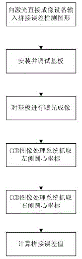
[0026] A method for detecting an imaging position error of a laser direct imaging device specifically includes the following steps:

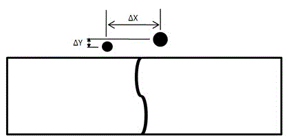
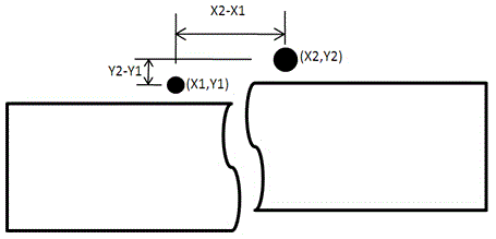
[0027] Step 1: The operator inputs a splicing error detection pattern to the laser direct imaging device. The splicing error detection pattern includes two circles with different diameters, where the center distance △x in the X direction is 3mm, and The distance between the centers of the circles △y is 0.2mm, the diameter of the left circle is 0.5mm, and the diameter of the right circle is 2mm, see figure 2 ;

[0028] Step 2: In a yellow light environment, a substrate is placed on the exposure workbench of the laser direct imaging device, and the substrate is a PCB board covered with a layer of photosensitive dry film;

[0029] Step 3: Under the environment of yellow light, the laser generated by the laser head of the laser direct imaging device is directly projected on the substrate according to the shape of the splicing error detection patte...

Embodiment 2

[0034] A method for detecting an imaging position error of a laser direct imaging device specifically includes the following steps:

[0035] Step 1: The operator inputs a splicing error detection pattern to the laser direct imaging device. The splicing error detection pattern includes two circles with different diameters, where the center distance △x in the X direction is 0.5mm, The distance between the center of the circle △y is 0mm, the diameter of the left circle is 0.1mm, and the diameter of the right circle is 0.2mm;

[0036] Step 2: In a yellow light environment, a substrate is placed on the exposure workbench of the laser direct imaging device, and the substrate is a PCB board covered with a layer of photosensitive dry film;

[0037] Step 3: Under the environment of yellow light, the laser generated by the laser head of the laser direct imaging device is directly projected on the substrate according to the shape of the splicing error detection pattern entered in step 1,...

Embodiment 3

[0042] A method for detecting an imaging position error of a laser direct imaging device specifically includes the following steps:

[0043] Step 1: The operator inputs a splicing error detection pattern to the laser direct imaging device. The splicing error detection pattern includes two circles with different diameters, where the center distance △x in the X direction is 10mm, and The distance between the centers of the circles △y is 10mm, the diameter of the left circle is 5mm, and the diameter of the right circle is 4mm;

[0044] Step 2: In a yellow light environment, a substrate is placed on the exposure workbench of the laser direct imaging device, and the substrate is a PCB board covered with a layer of photosensitive dry film;

[0045] Step 3: Under the environment of yellow light, the laser generated by the laser head of the laser direct imaging device is directly projected on the substrate according to the shape of the splicing error detection pattern entered in step ...


PUM

PropertyMeasurementUnit
diameteraaaaaaaaaa
diameteraaaaaaaaaa
diameteraaaaaaaaaa

Abstract

The invention provides a method for detecting an imaging position error of laser direct imaging equipment. The method comprises the following steps: inputting a stitching error detection graph into the laser direct imaging equipment; carrying out imaging on a substrate covered with a photosensitive dry film through a spatial light modulator; respectively grabbing center coordinates at two sides of the graph stitching position through a charge coupled device (CCD) image processing system of the laser direct imaging equipment; and calculating the error between the coordinates at two sides in X and Y directions, wherein the error is the stitching error. According to the method, the chemical development and microscope measurement steps are omitted; and the detection efficiency and accuracy are greatly improved.

Description

technical field [0001] The invention relates to the technical field of printed circuit board pattern transfer, in particular to a method for detecting imaging position errors of laser direct imaging equipment. Background technique [0002] For the field of printed circuit board processing, especially the manufacture of high-precision HDI boards and packaging substrates, image transfer equipment is undoubtedly the core part. [0003] At present, there are two types of printed circuit board (PCB) image transfer equipment: traditional projection exposure equipment and laser direct imaging equipment (LDI). The graphics of the traditional projection exposure equipment have been printed on the film film, and the film film is irradiated with ultraviolet rays to transfer the figure to the PCB with a photosensitive dry film on the surface. After the dry film is exposed, the unexposed part of the dry film is dissolved by a chemical solution. In the laser direct imaging equipment, the...

Claims


Application Information

Patent Timeline
Patent Type & Authority Applications(China)
IPC IPC(8): G03F7/20
Inventor 陆敏婷
Owner HEFEI CHIP FOUND MICROELECTRONICS EQUIP CO LTD
Why Eureka
Try Eureka