Storage unit and manufacture method thereof

A technology of storage unit and manufacturing method, which is applied in semiconductor/solid-state device manufacturing, electrical components, electric solid-state devices, etc., can solve problems affecting the reliability of memory devices, etc., and achieve the effect of reducing program disturbance and avoiding program disturbance

Active Publication Date: 2015-11-25
MACRONIX INT CO LTD
View PDF3 Cites 2 Cited by
  • Summary
  • Abstract
  • Description
  • Claims
  • Application Information

AI Technical Summary

Problems solved by technology

Therefore, when a programming operation is performed on an adjacent memory, program disturbance may easily occur and affect the reliability of the memory device

Method used


Image

  • Storage unit and manufacture method thereof
  • Storage unit and manufacture method thereof
  • Storage unit and manufacture method thereof

Examples


Embodiment Construction

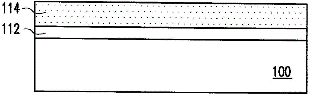
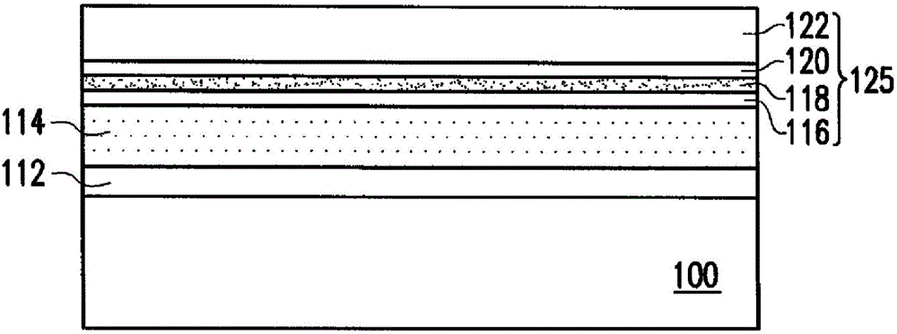
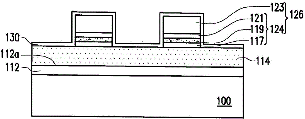
[0048] Figure 1A to Figure 1E It is a schematic cross-sectional view of the manufacturing process of the non-volatile memory device according to the first embodiment of the present invention.

[0049]Hereinafter, the first conductivity type is N-type, and the second conductivity type is P-type for illustration, but the present invention is not limited thereto. Those skilled in the art should understand that the first conductivity type can also be replaced by the P type, and the second conductivity type can be replaced by the N type. Wherein, N-type dopant is such as phosphorus or arsenic; P-type dopant is such as boron or boron difluoride (BF 2 ).

[0050] First, please refer to Figure 1A , forming an isolation structure 112 on the substrate 100 . The substrate 100 may be formed of at least one semiconductor material selected from the group consisting of Si, Ge, SiGe, GaP, GaAs, SiC, SiGeC, InAs and InP. The material of the isolation structure 112 is, for example, any su...


PUM


Abstract

The invention discloses a storage unit and a manufacture method thereof. The storage unit includes a base, two first conducting doping zones, a second conducting doping zone, two laminated structures and a first isolation structure. The first conducting doping zones are arranged in the base. The second conducting doping zones are arranged in the base between the two first conducting doping zones. The laminated structures are arranged on the base and cover the corresponding first conducting doping zone and a part of the second conducting doping zone respectively. Each laminated structure includes a charge storing layer. The first isolation structure fully covers and contacts with the bottom face of the first conducting doping zone and the bottom face of the second conducting doping zone.

Description

technical field [0001] The invention relates to a storage unit and a manufacturing method thereof. Background technique [0002] Memory is a semiconductor component used to store data or data. When the function of the computer microprocessor becomes stronger and stronger, the programs and calculations performed by the software become larger and larger, and the demand for memory becomes higher and higher. Among various storage components, non-volatile memory has the advantage that the stored data will not disappear after power failure, so many electrical products must have this type of memory to maintain the normal operation of the electrical product when it is turned on. [0003] Conventional nonvolatile memories have floating gates and control gates made of doped polysilicon. When the memory is programmed, electrons injected into the floating gate can be evenly distributed throughout the polysilicon floating gate. However, if the tunnel oxide layer under the polysilicon ...

Claims


Application Information

Patent Timeline
Patent Type & Authority Applications(China)
IPC IPC(8): H01L27/115H01L21/8247
Inventor 郑致杰颜士贵蔡文哲
Owner MACRONIX INT CO LTD
Why Eureka
Try Eureka