Transparent display device and manufacturing method thereof

A technology of transparent display and light-transmitting area, which is applied in the manufacture of semiconductor/solid-state devices, electric solid-state devices, semiconductor devices, etc. Effect

Inactive Publication Date: 2015-11-25
EVERDISPLAY OPTRONICS (SHANGHAI) CO LTD
View PDF4 Cites 19 Cited by
  • Summary
  • Abstract
  • Description
  • Claims
  • Application Information

AI Technical Summary

Problems solved by technology

It can be seen that the light transmittance of the transparent display screen in the prior art is relatively poor, and further, its display effect will be seriously affected.

Method used


Image

  • Transparent display device and manufacturing method thereof
  • Transparent display device and manufacturing method thereof
  • Transparent display device and manufacturing method thereof

Examples


no. 1 example

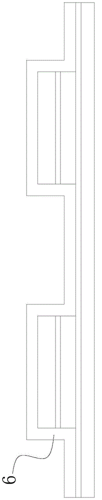
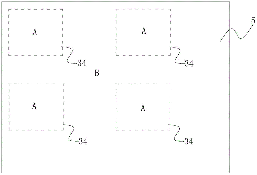
[0028] The transparent display includes a pixel area and a light-transmitting area. Wherein, a plurality of the pixel areas are arranged on the transparent display, and the pixel areas are used to emit light of three colors of RGB. The light-transmitting area is located between the pixel areas, that is, the area outside the pixel areas on the transparent display. The light-transmitting region is permeable to light, which directly affects the light-transmitting property and display effect of the transparent display.

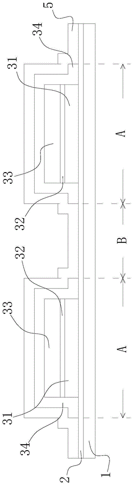
[0029] Please also see figure 2 and image 3 , which respectively show a longitudinal cross-sectional structural schematic view and a front view of the transparent display according to the first embodiment of the present invention. Such as figure 2 and image 3 As shown, in a preferred embodiment of the present invention, the transparent display includes a substrate 1, a buffer layer 2, and a plurality of organic electroluminescent devices. The substrate 1...

no. 2 example

[0042] See Figure 8 , which shows a schematic view of the vertical cross-sectional structure of the transparent display according to the second embodiment of the present invention. Such as Figure 8 shown, with the above figure 2 and image 3 The difference from the first embodiment shown is that the transparent display in this embodiment has a bottom emission structure, and the structure of the organic electroluminescent device is different from that in the first embodiment above. Specifically, the organic electroluminescent device of the transparent display includes: a thin film transistor 31', an anode 32', a light emitting layer 33' and a first cathode 34'.

[0043] The thin film transistor 31' is disposed on the pixel area of ​​the substrate 1. The thin film transistor 31' is preferably a low temperature polysilicon thin film transistor. The anode 32' is disposed on the substrate 1 and is located on the side of the thin film transistor 31'. The light-emitting laye...


PUM


Abstract

The invention discloses a transparent display device and a manufacturing method thereof. The transparent display device comprises a substrate and organic electroluminescence devices, wherein the substrate comprises a plurality of pixel regions and photic regions positioned among the pixel regions; the organic electroluminescence devices are arranged on the substrate, and are positioned on the pixel regions of the substrate; the organic electroluminescence devices comprise thin film transistors, pixel electrodes, luminescent layers, first opposite electrodes and second opposite electrodes; the thin film transistors are arranged on the pixel regions of the substrate; the pixel electrodes are arranged on the pixel regions of the substrate, and are electrically connected with the thin film transistors; the luminescent layers are arranged on the pixel electrodes; the first opposite electrodes are arranged on the pixel regions of the substrate, and are positioned above the thin film transistors and the luminescent layers; the second opposite electrodes are arranged above the pixel regions and the photic regions, the second opposite electrodes in the pixel regions are positioned above the first opposite electrodes, and the second opposite electrodes are used for electrically connecting the first opposite electrodes. According to the transparent display device disclosed by the invention, the light transmission and transparency of the transparent display device can be greatly improved.

Description

technical field [0001] The invention relates to the field of semiconductor devices, in particular to a transparent display. Background technique [0002] Compared with many display panels, OLED panels have become the only carrier for the development of transparent display technology due to their many advantages such as active light emission, high contrast, no viewing angle limitation, and unique device structure. [0003] Existing transparent displays are roughly divided into two structures, one is a bottom emission structure, and the other is a top emission structure. Generally, whether in a transparent display with a bottom-emitting structure or a top-emitting structure, an ordinary mask (not a high-precision mask) is generally used for full-screen cathode evaporation. See figure 1 , which shows a schematic view of a vertical cross-sectional structure of a transparent display in the prior art. Such as figure 1 As shown, taking a transparent display with a top-emission ...

Claims


Application Information

Patent Timeline
Patent Type & Authority Applications(China)
IPC IPC(8): H01L27/32H01L51/52H01L51/56
Inventor 熊娜娜徐小丽李艳虎
Owner EVERDISPLAY OPTRONICS (SHANGHAI) CO LTD
Why Eureka
Try Eureka