Fabrication method of superluminescent diode chip and fabricated light emitting diode chip

A superluminescence and diode technology, applied in diodes, electrical components, circuits, etc., can solve the problems of increased system volume, unfavorable integration, and increased cost, and achieve the effects of high output power, increased output, and reduced requirements

Active Publication Date: 2015-11-25
FUJIAN INST OF RES ON THE STRUCTURE OF MATTER CHINESE ACAD OF SCI
View PDF5 Cites 13 Cited by
  • Summary
  • Abstract
  • Description
  • Claims
  • Application Information

AI Technical Summary

Problems solved by technology

Therefore, in the actual application process, it is usually necessary to additionally use polarization-maintaining fiber or other polarization control devices, which increases the cost of device application and increases the size of the system, which is not conducive to integration.

Method used


Image

  • Fabrication method of superluminescent diode chip and fabricated light emitting diode chip
  • Fabrication method of superluminescent diode chip and fabricated light emitting diode chip
  • Fabrication method of superluminescent diode chip and fabricated light emitting diode chip

Examples


Embodiment Construction

[0031] In order to make the object, technical solution and advantages of the present invention clearer, the present invention will be described in further detail below in conjunction with specific embodiments and with reference to the accompanying drawings. However, those skilled in the art know that the present invention is not limited to the drawings and the following embodiments.

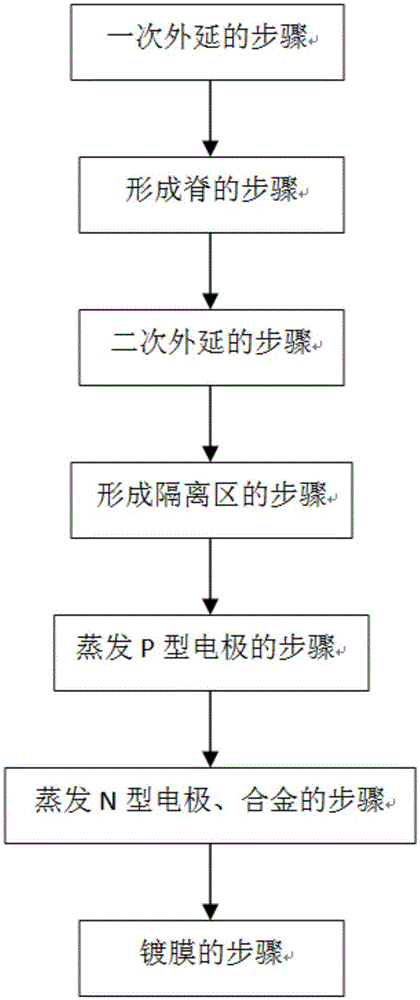
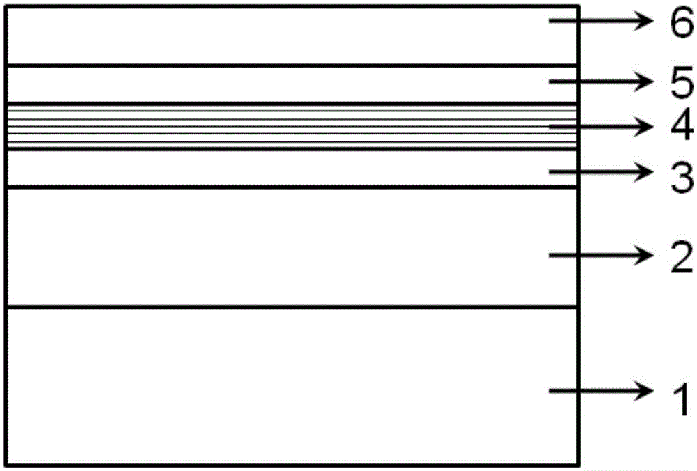
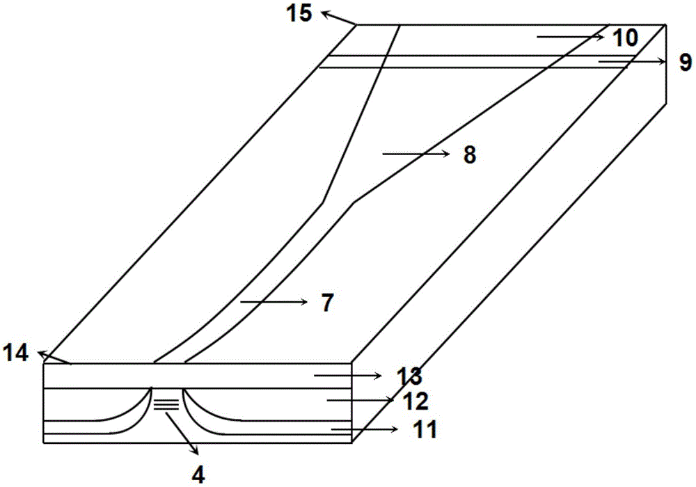
[0032] The invention relates to a method for preparing a superluminescent light-emitting diode chip, such as figure 1 Shown, this preparation method comprises the steps:

[0033]1. One-time epitaxy step: grow 1 μm N-InP buffer layer 2 on N-InP substrate 1 by MOCVD method, then grow 80nm InGaAsP lower confinement layer 3 respectively, and then alternately grow 3 tensile strains of 1.1% and two InGaAsP quantum wells with a compressive strain of 1.2%, the thicknesses of the tensile strain well and the compressive strain well are respectively 10nm and 5nm, the PL peak wavelengths are both 1300nm, an...


PUM

PropertyMeasurementUnit
thicknessaaaaaaaaaa
thicknessaaaaaaaaaa
thicknessaaaaaaaaaa

Abstract

The invention relates to a fabrication method of a superluminescent diode chip. The method comprises the following steps of one-step epitaxy, ridge forming, secondary epitaxy, isolation region forming, P-type electrode evaporation, N-type electrode evaporation, alloy and film coating. The invention also relates to a superluminescent diode chip fabricated according to the fabrication method. The chip fabricated according to the invention has the characteristics of low polarization, high output power and low spectrum corrugation.

Description

technical field [0001] The invention relates to a light-emitting diode chip, in particular to a method for preparing a super-radiant light-emitting diode chip and the prepared light-emitting diode chip. Background technique [0002] Superluminescent Diodes (SLD) is a semiconductor light-emitting device with wide spectrum, weak time coherence, high output power, and high efficiency. Its optical properties are between semiconductor laser LD and light-emitting diode LED. Wider luminescence spectrum and shorter coherence length, and higher output power than LED, its main advantages are wide spectrum and large output power; it is widely used in fiber optic gyroscope, fiber optic sensing, optical coherence tomography, etc. field. [0003] In the application fields of high-precision fiber optic gyroscopes and fiber optic sensors, in addition to high output power and wide spectrum, the polarization insensitivity of SLD is very important. On the other hand, the large output power c...

Claims


Application Information

Patent Timeline
Patent Type & Authority Applications(China)
IPC IPC(8): H01L33/00H01L33/06
CPCH01L33/0045H01L33/0062H01L33/06
Inventor 薛正群周东豪王凌华林琦林中晞陈阳华苏辉
Owner FUJIAN INST OF RES ON THE STRUCTURE OF MATTER CHINESE ACAD OF SCI
Why Eureka
Try Eureka