
Method for solving hard mask layer silicon nitride residue on dual active region graphic wafer

A technology of silicon nitride residue and hard mask layer, which is applied in the direction of radiation control devices, etc., can solve the problem of large height difference of silicon nitride mask layer, etc.

Inactive Publication Date: 2015-12-02
SHANGHAI HUALI MICROELECTRONICS CORP
View PDF3 Cites 0 Cited by
  • Summary
  • Abstract
  • Description
  • Claims
  • Application Information

AI Technical Summary

Problems solved by technology

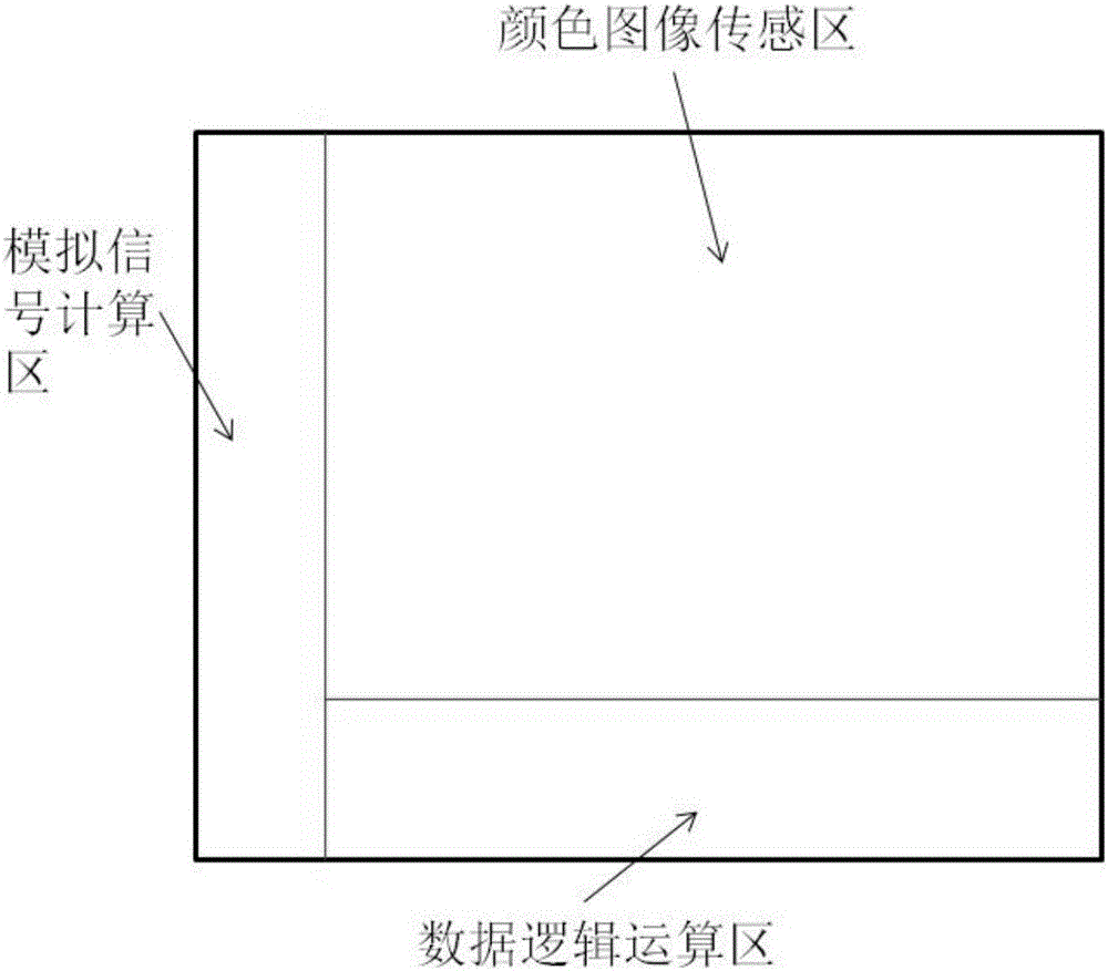
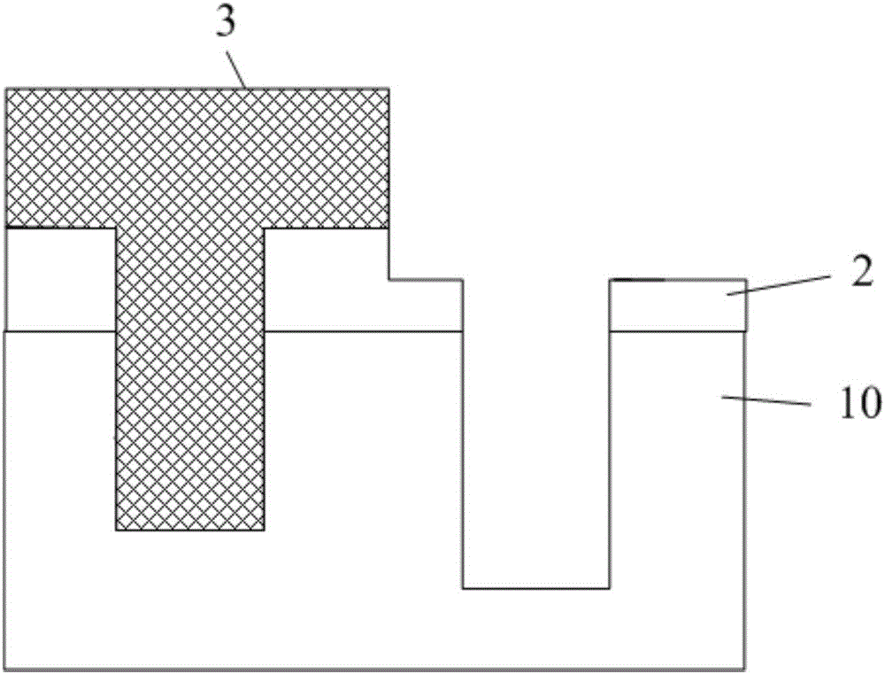
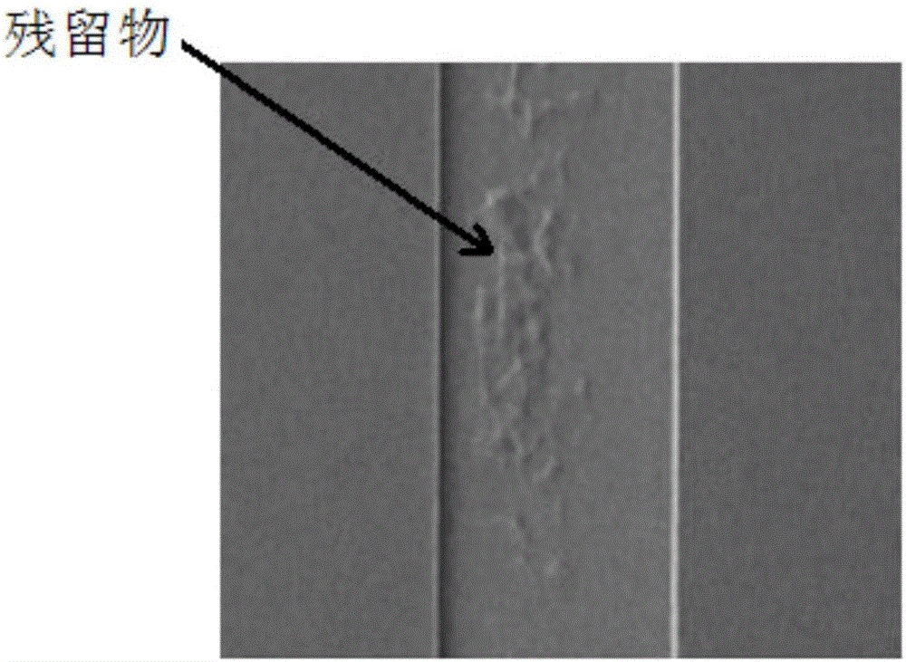
Due to the existence of this special structure on the wafer, if there is a slight deviation in the production process such as etching and grinding, resulting in a large difference in the height of the silicon nitride mask layer, it will lead to a large number of defects.

Method used


Image

  • Method for solving hard mask layer silicon nitride residue on dual active region graphic wafer
  • Method for solving hard mask layer silicon nitride residue on dual active region graphic wafer
  • Method for solving hard mask layer silicon nitride residue on dual active region graphic wafer

Examples


Embodiment Construction

[0026] In order to make the content of the present invention clearer and easier to understand, the content of the present invention will be described in detail below in conjunction with specific embodiments and accompanying drawings.

[0027] Figure 4 to Figure 9 Each step of the method for solving the residual silicon nitride on the dual-type active region pattern wafer according to the preferred embodiment of the present invention is schematically shown.

[0028] Such as Figure 4 to Figure 9 As shown, the method for solving the residual silicon nitride on the double-type active region pattern wafer according to the preferred embodiment of the present invention includes:

[0029] First step: growing different first hard mask layers 20 and second hard mask layers 30 sequentially on the wafer substrate 10 (for example, a silicon substrate), such as Figure 4 shown;

[0030] Wherein, both the first hard mask layer 20 and the second hard mask layer 30 have relatively large s...


PUM


Abstract

The invention provides a method for solving hard mask layer silicon nitride residue on a dual active region graphic wafer. The method includes the step that a first hard mask layer and a second hard mask layer which are different grow in order on a wafer substrate. Patterns of the first hard mask layer and the second hard mask layer are formed through lithography and etching technologies, and a first type of groove and a second type of groove are formed in the wafer substrate. A photoresistive agent is coated to cover the first type of groove, and the second type of groove is exposed. The second type of groove exposed by the photoresistive agent is further etched, so that the depth of the second type of groove in the wafer substrate is deepened. The depth of the second type of groove in the wafer substrate is more than that of the first type of groove in the wafer substrate. The photoresistive agent is removed, and then the second hard mask layer is removed.

Description

technical field [0001] The present invention relates to the field of semiconductor manufacturing, and more specifically, the present invention relates to a method for solving the residue of silicon nitride on the hard mask layer on the dual-type active area pattern wafer, which can optimize the production process of large-scale integrated circuits. Different active region depth structures. Background technique [0002] Advanced integrated circuit manufacturing processes often contain hundreds of processes, and the main process modules can be divided into several major parts such as photolithography, etching, ion implantation, film growth and cleaning. The designed circuit is transferred to the wafer through photolithography and etching processes, and then ion implantation technology is used to implant different concentrations and types of ions into the active area of ​​the wafer to form field effect crystal devices with different electrical properties. . [0003] With the ...

Claims


Application Information

Patent Timeline
IPC IPC(8): H01L27/146
Inventor 倪棋梁陈宏璘龙吟
Owner SHANGHAI HUALI MICROELECTRONICS CORP
Learn More