Laser cutting method for sapphire substrate LED chip

A technology of LED chips and sapphire substrates, applied in laser welding equipment, welding equipment, metal processing equipment, etc., can solve the problem of low yield, improve the cutting yield and reduce the phenomenon of oblique cracking

Inactive Publication Date: 2015-12-09
SHANDONG INSPUR HUAGUANG OPTOELECTRONICS
View PDF7 Cites 9 Cited by
  • Summary
  • Abstract
  • Description
  • Claims
  • Application Information

AI Technical Summary

Problems solved by technology

This method has a lower yield rate for chips with thicker sapphire substrates

Method used


Image

  • Laser cutting method for sapphire substrate LED chip
  • Laser cutting method for sapphire substrate LED chip

Examples


Embodiment Construction

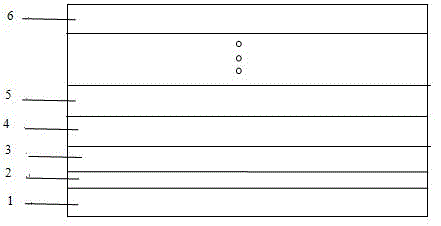
[0026] The cutting method of the sapphire substrate LED chip of the present invention is suitable for LED chips with a thickness ≥ 130 μm, comprising the following steps:

[0027] (1) Paste the LED chip on the white film 1 of SPV-224S type, the epitaxial layer 2 and the electrode surface of the LED chip are in contact with the white film 1, and the sapphire substrate is facing upward, and placed on the invisible cutting machine workbench.

[0028] (2) Set the focus of the stealth cutting laser so that the stealth cutting laser acts on the inside of the chip, close to the bottom, and cut at a distance of 50-100 μm from the bottom to form the first modified layer 3 .

[0029] Stealth cutting laser power 180-300mW (laser frequency 50KHz). The cutting speed is 250-550mm / s.

[0030] The modified layer refers to the use of a laser with a certain wavelength to focus on the inside of the workpiece material to form a starting point for division. The part around the starting point that...


PUM

PropertyMeasurementUnit
depthaaaaaaaaaa
thicknessaaaaaaaaaa

Abstract

A laser cutting method for a sapphire substrate LED chip comprises the following steps: (1) cutting at the position close to the bottom inside the LED chip under the invisible cutting laser action, so as to form a first modified layer; (2), enabling laser to focus at the upper part of the first modified layer through increasing the laser focus depth, and cutting to form a second modified layer connected with the first modified layer vertically; (3) increasing the laser focus depth again to form a third modified layer, forming N modified layers through similar operation, and enabling stress released by the last modified layer to extend to the surface of the chip to form cracks, wherein the N is greater than or equal to 2; (4) applying external force to the LED chip wafer in the directions of the cracks, so as to divide the chip into independent light-emitting units. When the method is used for cutting a thicker wafer of a sapphire substrate, the cutting yield can be effectively increased, and inclined sapphire cracks are reduced.

Description

technical field [0001] The invention relates to a laser cutting method for a sapphire substrate LED (Light Emitting Diode, light emitting diode) chip, belonging to the technical field of LED chip cutting. Background technique [0002] Since Nichia successfully developed the GaN-based blue LED in 1991, its development speed can be said to be changing with each passing day. LED has become a new generation of lighting source in the 2l century due to its low energy consumption, long life, green environmental protection, fast response time and other advantages. With the maturity of the III-V semiconductor process, the development of LED chips continues to develop in the direction of high efficiency and high brightness. Traditional chip cutting methods such as diamond scribing and grinding wheel sawing have gradually become outdated due to their low efficiency and low yield, and cannot meet the needs of modern production. At present, laser cutting is gradually replacing tradition...

Claims


Application Information

Patent Timeline
Patent Type & Authority Applications(China)
IPC IPC(8): B23K26/53B23K26/402
Inventor 王贤洲彭璐李法健徐现刚
Owner SHANDONG INSPUR HUAGUANG OPTOELECTRONICS
Why Eureka
Try Eureka