LED chiplet and LED chip invisible cutting method

A technology of LED chip and stealth cutting, which is applied in the manufacturing of electrical components, electric solid-state devices, semiconductor/solid-state devices, etc., can solve the problems of low chip cutting yield, increased electrical failure rate of LED chips, and reduced cutting yield. , to reduce the phenomenon of substrate skew cracking, reduce the line width of the cutting track, and improve the cutting yield.

Inactive Publication Date: 2019-09-27
XIAMEN SANAN OPTOELECTRONICS TECH CO LTD
View PDF5 Cites 9 Cited by
  • Summary
  • Abstract
  • Description
  • Claims
  • Application Information

AI Technical Summary

Problems solved by technology

[0002] At present, the LED chip is divided into independent LED chips, which is usually completed by forming a single laser scratch inside the substrate through invisible cutting, and then splitting. However, it is easy to cut and grind thicker chips (thickness is generally greater than 150 μm) The following situations occur: (1) Due to the low laser energy used in stealth dicing, twin cells or even multiple cells are prone to occur, and the core particle cutting yield is low; (2) The chip can be split normally, but the laser cutting position and There is a large deviation in the crack position, and the oblique crack is serious. As shown in Figure (1), the line width of the cutting line needs to be increased, otherwise it is easy to damage the light-emitting area and reduce the brightness; and increasing the line width of the cutting line will cause Reduce the output of LED chips on a single wafer
[0003] In some cases, there is a dicing process that uses stealth dicing on the back and the cutting depth is greater than 1 / 2 of the chip thickness to solve technical problems such as low yield and low brightness caused by oblique cracks.
However, the closer the stealth cutting position is to the epitaxial layer, the electrical failure rate of the LED chip will increase. Therefore, a smaller laser energy must be used to reduce the electrical abnormality, which will lead to an increase in the number of twins or even multiples of the chip, and a decrease in the cutting yield.
[0004] In addition, in order to ensure the normal photoelectric parameters of the chip and take into account the appearance yield after chip splitting, the stealth dicing technology usually applied to LED requires a proper combination of stealth dicing laser energy and laser focus position, so that the laser ablation marks on the side of the chip after splitting can be maintained at Within a certain range, the side of the chip is relatively smooth, so the light emitted from the side of the core particle cannot be collected effectively

Method used


Image

  • LED chiplet and LED chip invisible cutting method
  • LED chiplet and LED chip invisible cutting method
  • LED chiplet and LED chip invisible cutting method

Examples


Embodiment 1

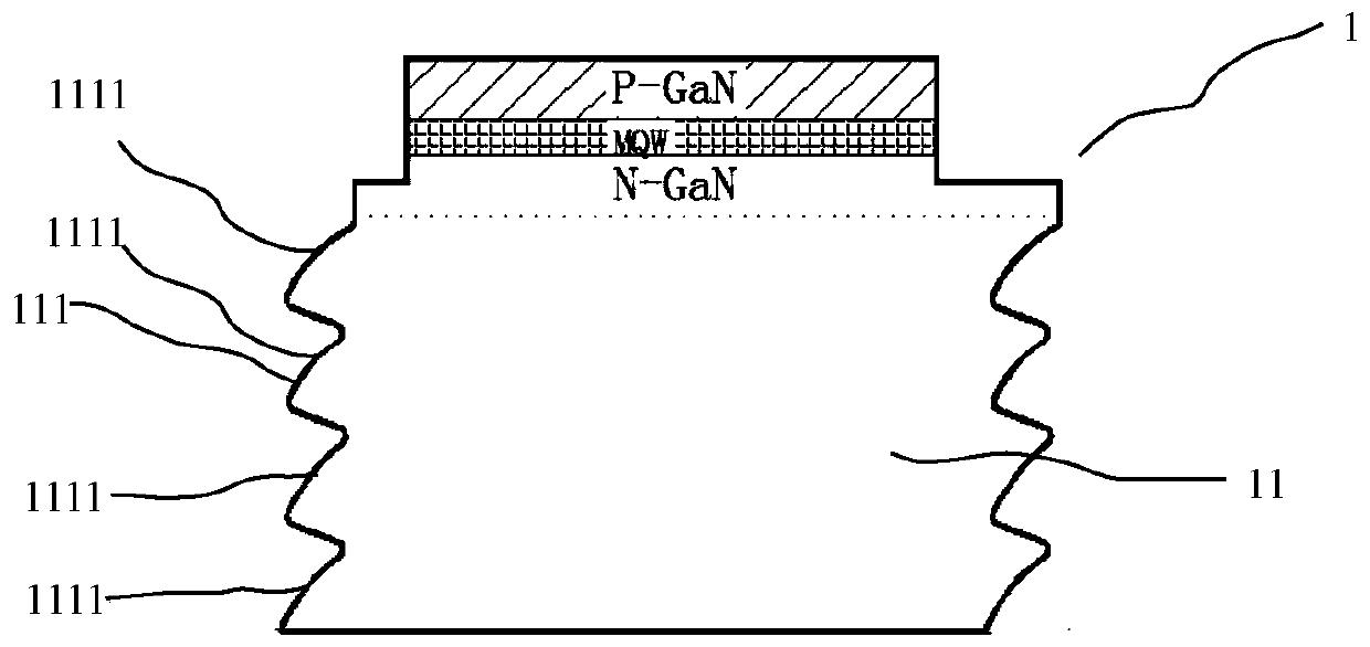
[0054] Such as figure 2 As shown, a LED chip 1, the side surface of the substrate 11 of the LED chip 1 (in this specific embodiment, the substrate 11 is a sapphire substrate, and the c-plane surface of the sapphire substrate grows an epitaxial layer) 111 has a plurality of spaced laser scratches 1111 along the thickness direction of the substrate 11. In this specific embodiment, the number of laser scratches 1111 is four, but it is not limited thereto. In other embodiments, the number of laser scratches 1111 The number can be set according to the thickness of the substrate 11, such as 3, 5 or more than 5 and so on.

[0055] The side surface 111 of the substrate 11 is arranged up and down sequentially along the thickness direction of the substrate 11 (approximately wavy), and the multiple laser scratches 1111 on the same side surface 111 of the substrate 11 are located on the same side of the substrate 11. In a plane parallel to the thickness direction, that is, in the same v...

Embodiment 3

[0064] This embodiment provides a stealth cutting method for LED chips, including:

[0065] In step S0, a full-structure LED chip 3 is produced according to the LED chip process, including forming an epitaxial layer 32 and a dicing line 33 on the c-plane surface of the sapphire substrate 31; and then grinding and thinning the LED chip 3 to a predetermined thickness , this example is 200μm, such as Figure 7 and 8 shown.

[0066] Step S11, first adopt invisible cutting on the back side, move the laser focusing point to the distance a1 from the back side of the LED chip 3 along the Y direction, a1 is 10 μm-30 μm, adjust the laser energy to 0.01W-0.5W, and adjust the laser frequency to 1KHz-100KHz , adjust the moving speed of the stage to 1mm / s-800mm / s, so that it forms a row of holes 34 with a distance D of 3μm-20μm and a diameter d of 1μm-4μm, forming the first laser scratch 341, as Figure 9 shown.

[0067] Step S12, then move the focus of the laser to the distance a1+a2 f...

Embodiment 5

[0085] The difference between this embodiment and Embodiment 1 is: this embodiment adopts a stealth cutting machine with four laser heads, and the four laser beams of the four laser heads respectively form the first laser scratch to the fourth laser scratch at the same time ,Such as Figure 13 As shown, four laser scratches are completed at one time, which increases the output of the machine.

[0086] Of course, in other embodiments, the number of laser heads can be determined according to the number of laser scratches.


PUM


Abstract

The present invention relates to the field of LED chip technology, and particularly relates to an LED chiplet and an LED chip invisible cutting method. The LED chiplet is disclosed, wherein the side surface of a substrate of the LED chiplet is provided with a plurality (three or more) of spaced laser scratches along the thickness direction of the substrate, and the side surface of the substrate is arranged in an up-and-down manner along the thickness direction of the substrate. The method is also provided, including a step S1) of forming a plurality of (three or more) laser scratches spaced along the thickness direction of the substrate inside the substrate in a cutting passage by adopting invisible cutting. According to the LED chiplet and the method, the yield of chiplet cutting is increased, substrate inclination is reduced, and the width of cutting passage lines can be reduced, thus increasing the yield from one chip. Side light extraction is increased, the light emitting angle is increased and forward-direction light is increased, thus increasing the brightness of the chiplet.

Description

technical field [0001] The invention belongs to the technical field of LED chips, and in particular relates to an LED chip and an invisible cutting method for LED chips. Background technique [0002] At present, the LED chip is divided into independent LED chips, which is usually completed by forming a single laser scratch inside the substrate through invisible cutting, and then splitting. However, it is easy to cut and grind thicker chips (thickness is generally greater than 150 μm) The following situations occur: (1) Due to the low laser energy used in stealth dicing, twin cells or even multiple cells are prone to occur, and the core particle cutting yield is low; (2) The chip can be split normally, but the laser cutting position and There is a large deviation in the crack position, and the oblique crack is serious. As shown in Figure (1), the line width of the cutting line needs to be increased, otherwise it is easy to damage the light-emitting area and reduce the brightn...

Claims


Application Information

Patent Timeline
Patent Type & Authority Applications(China)
IPC IPC(8): H01L21/78H01L27/15H01L33/00
CPCH01L21/78H01L33/005H01L27/156H01L33/0095H01L33/20H01L33/24
Inventor 陈功林素慧许圣贤彭康伟洪灵愿何敏游张家宏
Owner XIAMEN SANAN OPTOELECTRONICS TECH CO LTD
Why Eureka
Try Eureka