Mask and fabrication method of thin film transistor
A mask, light-transmitting area technology, applied in the manufacture of semiconductor/solid-state devices, photoengraving process of patterned surface, originals for opto-mechanical processing, etc. , to avoid the effect of short circuit
- Summary
- Abstract
- Description
- Claims
- Application Information
AI Technical Summary
Problems solved by technology
Method used
Image

Examples
Embodiment 1
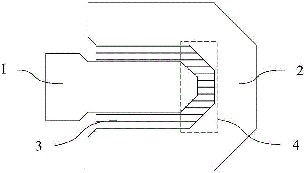
[0039] An embodiment of the present invention provides a mask, which may specifically be a single-slit mask, a halftone mask (HalfToneMask, HTM for short), or a gray scale mask (HalfToneMask, GTM for short). In this embodiment, a single slit mask is taken as an example for illustration, as figure 2 and image 3 As shown, the single slit mask includes an opaque region, a partially transparent region (single slit region) and a fully transparent region.
[0040] The opaque area includes a source pattern 101 and a drain pattern 102 corresponding to the source and drain of the thin film transistor, and may also include various patterns corresponding to data lines and other lines in the edge area. The fully light-transmitting area corresponds to patterns other than traces such as sources, drains, channels, and data lines of the thin film transistors.
[0041] The partially transparent region includes a channel pattern corresponding to the channel of the thin film transistor. The...
Embodiment 2
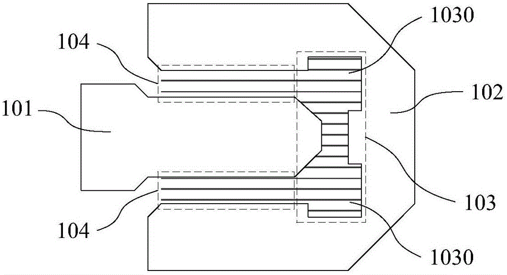
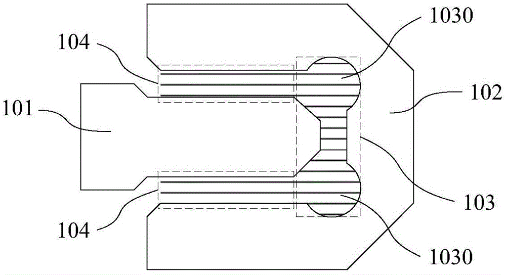
[0046] Such as Figure 4 and Figure 5 As shown, the embodiment of the present invention provides a single-slit mask, which is basically the same as the first embodiment, including an opaque region, a partially transparent region (single slit region) and a fully transparent region. Among them, the opaque area includes graphics such as source pattern 201 and drain pattern 202; the fully light-transmitting area corresponds to patterns other than the source, drain, channel, and data lines of the thin film transistor; the partially light-transmitting area It includes a horseshoe-shaped channel pattern, and the width of the bent portion 203 of the channel pattern is greater than the width of the straight extension portion 204 .
[0047] The difference between this embodiment and the first embodiment is that, in this embodiment, a notch 2030 is formed on the inner edge of the bent portion 203 , so that the width of the bent portion 203 is greater than the width of the straight exte...
Embodiment 3
[0050] An embodiment of the present invention provides a method for manufacturing a thin film transistor, which can be applied in the manufacturing process of an array substrate using a 4-step patterning process. As a preferred solution, the width of the channel of the thin film transistor is less than 4 microns.
[0051] The manufacturing method includes:
[0052] S1: forming a gate by using a patterning process.
[0053] This step can be performed by using a common mask and a conventional patterning process, and will not be described in detail here.
[0054] In addition, after this step is completed, a gate insulating layer needs to be formed on the gate.
[0055] S2: Forming source, drain and channel by patterning process. Specifically include:
[0056] S21: sequentially forming a semiconductor layer and a source-drain metal layer on the gate insulating layer.
[0057] S22: Coating a photoresist on the source-drain metal layer, and using the mask provided in the first ...
PUM
| Property | Measurement | Unit |
|---|---|---|
| Width | aaaaa | aaaaa |
| Width | aaaaa | aaaaa |
Abstract
Description
Claims
Application Information
 - Generate Ideas
- Intellectual Property
- Life Sciences
- Materials
- Tech Scout
- Unparalleled Data Quality
- Higher Quality Content
- 60% Fewer Hallucinations
Browse by: Latest US Patents, China's latest patents, Technical Efficacy Thesaurus, Application Domain, Technology Topic, Popular Technical Reports.
© 2025 PatSnap. All rights reserved.Legal|Privacy policy|Modern Slavery Act Transparency Statement|Sitemap|About US| Contact US: help@patsnap.com