Drive circuit for thin-film transistor liquid crystal display

A liquid crystal display and thin film transistor technology, applied in static indicators, instruments, etc., can solve problems such as excessive power consumption, and achieve the effects of reducing power consumption, saving electric energy, and flexible control methods

Inactive Publication Date: 2015-12-09
AU OPTRONICS CORP
View PDF0 Cites 10 Cited by
  • Summary
  • Abstract
  • Description
  • Claims
  • Application Information

AI Technical Summary

Problems solved by technology

[0005] In view of this, how to design a driving circuit of a thin film transistor liquid crystal display, or improve the existing driving circuit, to overcome the above-mentioned defects of excessive power consumption in the prior art, is an urgent problem to be solved by relevant technical personnel in the industry. subject

Method used


Image

  • Drive circuit for thin-film transistor liquid crystal display
  • Drive circuit for thin-film transistor liquid crystal display
  • Drive circuit for thin-film transistor liquid crystal display

Examples


Embodiment Construction

[0031] In order to make the technical content disclosed in this application more detailed and complete, reference may be made to the drawings and the following various specific embodiments of the present invention, and the same symbols in the drawings represent the same or similar components. However, those skilled in the art should understand that the examples provided below are not intended to limit the scope of the present invention. In addition, the drawings are only for schematic illustration and are not drawn according to their original scale.

[0032] The specific implementation manners of various aspects of the present invention will be further described in detail below with reference to the accompanying drawings.

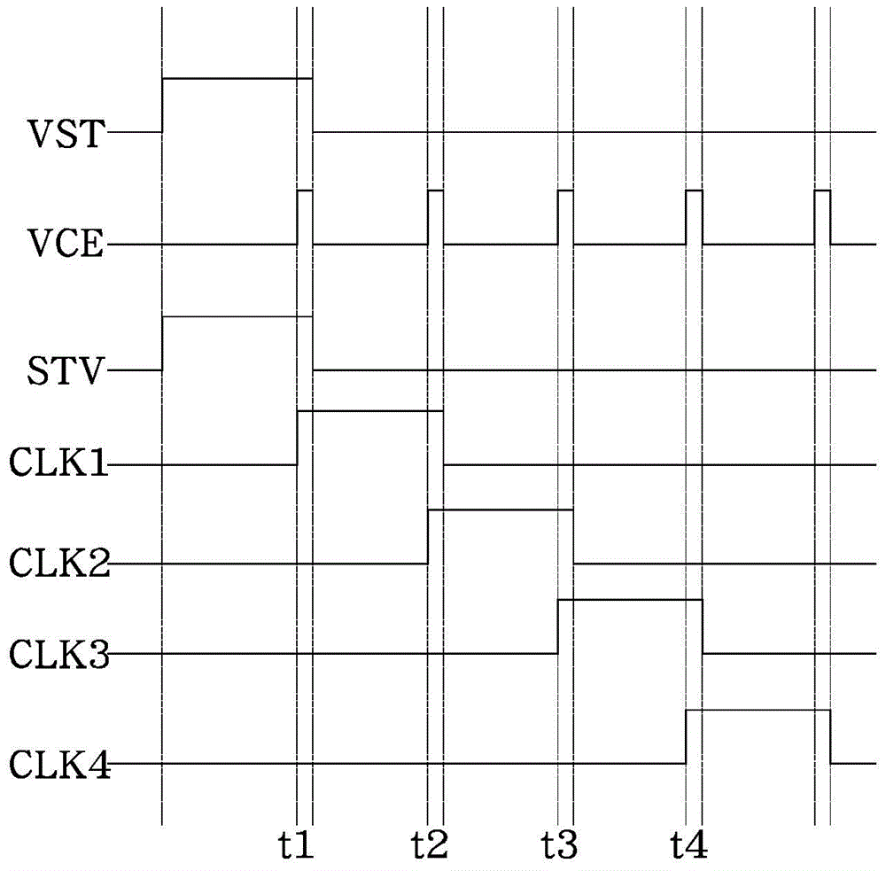
[0033] figure 1 A control timing diagram of key signals of a driving circuit for a thin film transistor liquid crystal display in the prior art is shown.

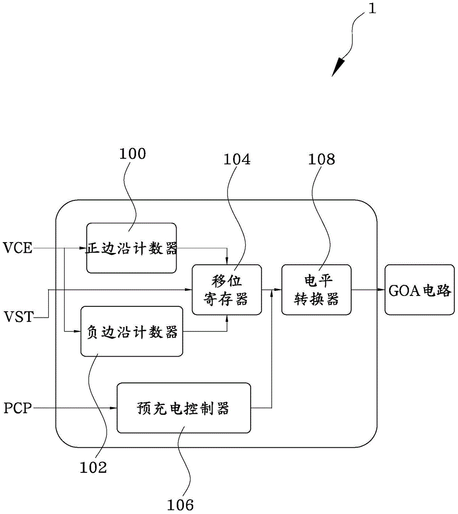
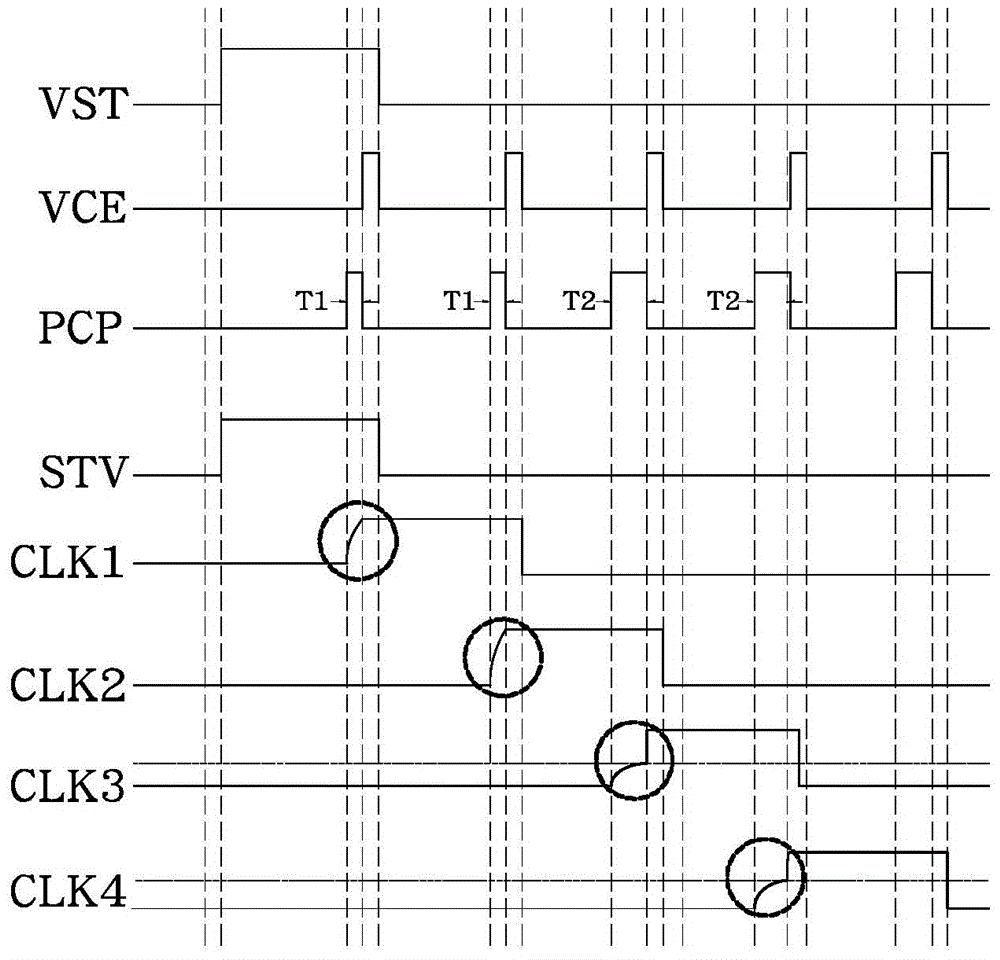
[0034] refer to figure 1, VST represents the gate start signal, VCE represents the clock enable si...


PUM


Abstract

Provided in the invention is a drive circuit for a thin-film transistor liquid crystal display. The drive circuit comprises a positive edge counter, a negative edge counter, a shift register, a pre-charging controller, and a lever shifter. To be specific, the positive edge counter is used for outputting a first control signal; the negative edge counter is used for outputting a second control signal; the shift register is used for receiving a gate starting signal and outputting a plurality of clock signals according to the first and second control signals; the pre-charging controller is used for outputting a pre-charging pulse width modulation signal; and the level shifter is used for carrying out a pre-charging operation on rising edges of at least parts of clock signals according to the pre-charging pulse width modulation signal. Compared with the prior art, the pre-charging controller outputs the pre-charging pulse width modulation signal; and thus the level shifter can carry out the pre-charging operation on rising edges of at least parts of clock signals. Therefore, the clock signals after pre charging can open the gate of the thin-film transistor in advance to charge a pixel, so that the pixel can be charged to an expected voltage potential rapidly; and thus the power consumption of the drive circuit can be reduced.

Description

technical field [0001] The invention relates to a thin film transistor liquid crystal display, in particular to a driving circuit for the thin film transistor liquid crystal display. Background technique [0002] In a thin film transistor liquid crystal display (ThinFilmTransistorLiquidCrystalDisplay, TFT-LCD), each pixel has a thin film transistor (ThinFilmTransistor, TFT), the gate of the thin film transistor is electrically connected to the scanning line in the horizontal direction, and the drain is electrically connected to the vertical scanning line. direction of the data line, and the source is electrically connected to a pixel electrode. If a sufficient positive voltage is applied to a scanning line in the horizontal direction, all the TFTs on the scanning line will be turned on, and at this time, the pixel electrode corresponding to the scanning line will be connected to the data line in the vertical direction, thereby connecting the data line The video signal volta...

Claims


Application Information

Patent Timeline
Patent Type & Authority Applications(China)
IPC IPC(8): G09G3/36
Inventor 温竣贵施鸿民
Owner AU OPTRONICS CORP
Why Eureka
Try Eureka