Interconnection material containing Yb and namometer Cu and formed by stacking of 3D chips

A technology of chip stacking and interconnection materials, applied in the direction of electrical components, electrical solid devices, circuits, etc., can solve problems such as shortage, achieve high service life, meet high reliability requirements, and resist deformation

Inactive Publication Date: 2015-12-16
XUZHOU NORMAL UNIVERSITY
View PDF7 Cites 2 Cited by
  • Summary
  • Abstract
  • Description
  • Claims
  • Application Information

AI Technical Summary

Problems solved by technology

The reliability of the three-dimensional packaging structure can be significantly improved by studying new interconnect materials, but there is currently a lack of relevant reports on this aspect

Method used


Image

  • Interconnection material containing Yb and namometer Cu and formed by stacking of 3D chips
  • Interconnection material containing Yb and namometer Cu and formed by stacking of 3D chips

Examples


Embodiment 1

[0018] A 3D chip stacked interconnection material containing Yb and nano-Cu is composed of: 0.01% of rare earth element Yb, 1% of nano-Cu particles, and the balance of In.

[0019] The service life of high-strength solder joints formed after bonding (170°C, 5MPa) is about 3300 thermal cycles (considering the experimental error), and the paste interconnection material has excellent solderability.

Embodiment 2

[0021] A 3D chip stacked interconnection material containing Yb and nano-Cu is composed of: 0.02% of rare earth element Yb, 2% of nano-Cu particles, and the balance of In.

[0022] The service life of the high-strength solder joints formed after bonding (200°C, 5MPa) is about 3500 thermal cycles (considering the experimental error), and the paste interconnection material has excellent solderability.

Embodiment 3

[0024] A 3D chip stacked interconnection material containing Yb and nano-Cu is composed of 0.5% of rare earth element Yb, 5% of nano-Cu particles, and the balance of In.

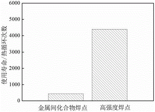
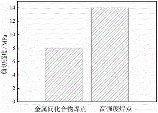
[0025] The service life of the high-strength solder joints formed after bonding (260°C, 10MPa) is about 4400 thermal cycles (considering the experimental error), and the paste interconnection material has excellent solderability.


PUM


Abstract

The invention discloses an interconnection material containing Yb and namometer Cu and formed by stacking of 3D chips, and belongs to the field of chip interconnection materials. In the interconnection material, the content of the rare earth element Yb is 0.01-0.5%, the content of nanometer Cu particles is 1-5%, and the remaining is In. Firstly, In-Yb intermediate alloy powder is prepared; secondly, the In-Yb powder, In powder, mixed rosin resin, a thixotropic agent, a stabilizing agent, an activity adjuvant and an activator are mixed and are fully stirred; and finally, the nanometer Cu particles are added, the paste interconnection material containing Yb and the nanometer Cu particles are fully stirred, precise screen printing and reflow welding technologies are adopted to prepare protruding points on the surfaces of chips, vertical interconnection of the chips in three-dimensional space is realized under certain pressure (1MPa-10Mpa) and temperature (170-260 DEG C) conditions, and high-intensity interconnection welding points are formed. The interconnection material is high in reliability and can be used for vertical packaging of chips packaged in three dimensions.

Description

technical field [0001] The invention relates to an interconnection material containing Yb and nanometer Cu for 3D chip stacking, and belongs to the field of chip interconnection materials. The interconnection material is mainly used in the field of three-dimensional packaging with high reliability requirements, and is a new type of interconnection material with high performance. Background technique [0002] Moore's Law is an important law for predicting the development of electronic industry technology, but with the increasing integration of a single chip, it seems that Moore's Law is difficult to continue to use, and the emergence of three-dimensional packaging technology directly determines the post-Moore era. It has also revolutionized the field of electronic packaging. Three-dimensional packaging, that is, stacking chips layer by layer in vertical space on the basis of two-dimensional packaging, can improve packaging density and product performance, reduce noise and en...

Claims


Application Information

Patent Timeline
Patent Type & Authority Applications(China)
IPC IPC(8): H01L23/532H01L21/768
Inventor 张亮郭永环孙磊
Owner XUZHOU NORMAL UNIVERSITY
Why Eureka
Try Eureka