Resistive random access memory with planar structure and manufacturing method thereof

A technology of resistive memory and planar structure, applied in the direction of electrical components, etc., to achieve the effect of simple method, saving raw material cost, and high mobility characteristics

Inactive Publication Date: 2015-12-16
FUDAN UNIV
View PDF4 Cites 9 Cited by
  • Summary
  • Abstract
  • Description
  • Claims
  • Application Information

AI Technical Summary

Problems solved by technology

[0002] With the further scaling down of the feature size of semiconductor devices, traditional flash memory technology will reach the limit of size

Method used


Image

  • Resistive random access memory with planar structure and manufacturing method thereof
  • Resistive random access memory with planar structure and manufacturing method thereof
  • Resistive random access memory with planar structure and manufacturing method thereof

Examples


Embodiment Construction

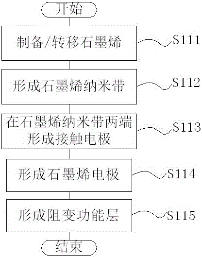
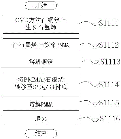
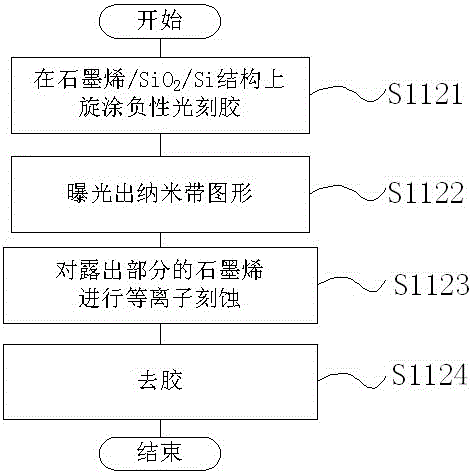
[0030] Embodiments of the present invention will be described in detail below with reference to the accompanying drawings, in which like elements are denoted by like reference numerals. The embodiments described below are exemplary, and in order to simplify the disclosure of the present invention, components and arrangements of specific examples are described below. Of course, these are only examples for the purpose of explaining the present invention and should not be construed as limiting the present invention. In addition, the present invention provides various specific examples of processes and materials, but the invention may be practiced without these specific details, as will be understood by those skilled in the art. Unless otherwise specified below, each part of the device can be implemented using processes and materials known in the art. Additionally, configurations described below in which a first feature is "on" a second feature may include embodiments where the f...


PUM


Abstract

The invention belongs to the technical field of resistive random access memories, and specifically discloses a resistive random access memory with a planar structure and a manufacturing method thereof. The resistive random access memory is provided with graphene electrodes formed at two ends of a resistive random functional layer, and low power consumption operation of the resistive random access memory is realized by utilizing high mobility of a graphene material. The resistive random access memory with the planar structure is favorable for observing the shape of a conductive filament and researching the mechanism of the resistive random access memory. Gaps with the size of dozens of nanometers are formed close to the middle of a graphene nano belt by adopting an electric joule heat fusing method, and then the graphene electrodes are formed. The resistive random functional layer is formed on the basis of the characteristic of lateral growth thereof in the graphene in an atomic layer deposition process. The method is simple and effective and reduces the cost of raw materials, and the size of the resistive random access memory can be adjusted.

Description

technical field [0001] The invention belongs to the technical field of resistive memory, and in particular relates to a resistive memory with a planar structure and a preparation method thereof. Background technique [0002] With the further proportional reduction of the feature size of semiconductor devices, the traditional flash memory technology will reach the limit of size. In order to further improve the performance of devices, technicians began to actively explore new structures, new materials, and new processes. In recent years, various new types of non-volatile memories have been developed rapidly. Among them, resistive RAM (RRAM) is receiving more and more attention in the industry due to its advantages such as simple structure, strong shrinkability, high density, long data retention time, three-dimensional integration, and compatibility with complementary metal oxide semiconductor (CMOS) processes. Attention, it is considered to be very likely to replace static r...

Claims


Application Information

Patent Timeline
Patent Type & Authority Applications(China)
IPC IPC(8): H01L45/00
Inventor 陈琳孙清清张卫
Owner FUDAN UNIV
Why Eureka
Try Eureka