Ceramic ring capable of changing shape and appearance of surface film of wafer

A technology of ceramic rings and wafers, applied in electrical components, semiconductor/solid-state device manufacturing, circuits, etc., can solve problems affecting wafer air flow, changes in plasma distribution, changes in gas distribution, etc., to achieve improved growth and reasonable structure , practical effect

Inactive Publication Date: 2015-12-23
PIOTECH CO LTD
View PDF4 Cites 7 Cited by
  • Summary
  • Abstract
  • Description
  • Claims
  • Application Information

AI Technical Summary

Problems solved by technology

During this process, the step part supporting the wafer is higher than the wafer, which will affect the flow of the gas flow at the edge of the wafer, and easily cause the gas distribution here to change, resulting in changes in the plasma distribution.

Method used


Image

  • Ceramic ring capable of changing shape and appearance of surface film of wafer
  • Ceramic ring capable of changing shape and appearance of surface film of wafer
  • Ceramic ring capable of changing shape and appearance of surface film of wafer

Examples


Embodiment 1

[0017] Embodiment 1 of the present invention occurs in the SiH4 process, the reaction source is SiH4 and N2O, and the hardware and substrate used in the experiment are as follows:

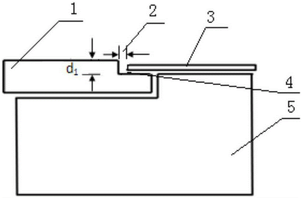
[0018] 1. Please refer to figure 1 , the groove depth of the ceramic ring used in this example is d 1 The ranges are 0.5mm-1.0mm and 1.0-1.5mm respectively, and the ceramic ring is on the stage for the support of the object to be processed.

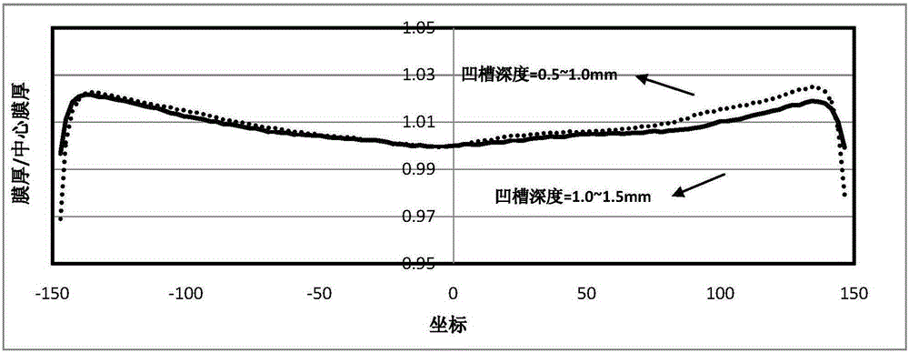
[0019] 2. The substrate used in this embodiment is a silicon wafer with a diameter of 300 mm and a thickness of 0.775 μm.

[0020] Please refer to figure 2 , which is a comparison of the deposition conditions of different ceramic ring step heights under the same process formulation. Taking the center of the silicon wafer as the origin, the x-axis is the coordinate (-147mm-147mm) along the radial direction of the silicon wafer at a distance of 3 mm from the edge of the silicon wafer, and the y-axis is the thickness of the film on the surface of the silicon ...

Embodiment 2

[0022] Embodiment 2 of the present invention occurs in the TEOS process, and the reaction source is TEOS and O 2 , the hardware and substrate used in the experiment are as follows:

[0023] 1. Please refer to figure 1 , the groove depth of the ceramic ring used in this example is d 1 The ranges are 0.5mm-1.0mm and 1.0mm-1.5mm respectively, and the ceramic ring is on the stage for the support of the object to be processed.

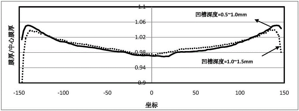
[0024] 2. The substrate used in this embodiment is a silicon wafer with a diameter of 300 mm and a thickness of 0.775 μm.

[0025] Please refer to image 3 , which is a comparison of the deposition conditions of different ceramic ring groove depths under the same process formulation. Taking the center of the silicon wafer as the origin, the x-axis is the coordinate (-147mm-147mm) along the radial direction of the silicon wafer at a distance of 3 mm from the edge of the silicon wafer, and the y-axis is the thickness of the film on the surface of the sili...


PUM

PropertyMeasurementUnit
thicknessaaaaaaaaaa
depthaaaaaaaaaa

Abstract

The invention provides a ceramic ring which can change the shape and appearance of a surface film of a wafer in a semiconductor plasma processing device. The ceramic ring is located on an objective table, and is used for bearing a to-be-machined wafer. An edge, supporting the step of the wafer, of the ceramic ring is at a right angle, and the height d1 of the step can be set differently. When a plasma air flow passes through the edge of the step, the height of the step exerts impact on the flowing of the air flow in a high-temperature process, thereby impacting the uniformity of a film layer. The ceramic ring can effectively adjust the air flow distribution at the step of the ceramic ring and the edge of the wafer, thereby impacting the uniformity of plasma distribution, and improving the growth condition of the edge film of the wafer. The ceramic ring is reasonable in structure, is practical and is easy to implement. The ceramic ring can be widely used in the technical field of semiconductor film deposition.

Description

technical field [0001] The invention relates to a wafer bearing ceramic ring for semiconductor coating equipment, which is mainly used in the normal temperature or high temperature process in the reaction chamber of the semiconductor coating equipment, and belongs to the application technical field of semiconductor thin film deposition. Background technique [0002] In existing plasma processing devices, the size of the circular groove of the ceramic ring used for wafer loading is fixed. Take away. During this process, the step part supporting the wafer is higher than the wafer, which will affect the flow of the gas flow at the edge of the wafer, and easily cause the gas distribution here to change, thereby causing the change of the plasma distribution. In the case of the above-mentioned uneven distribution of plasma, it is reflected in the plasma treatment process of semiconductors that it affects the thickness of the deposited film on the wafer, which will affect the morp...

Claims


Application Information

Patent Timeline
Patent Type & Authority Applications(China)
IPC IPC(8): H01L21/67H01L21/683
CPCH01L21/67H01L21/67213H01L21/683
Inventor 刘忆军杨艳戚艳丽宁建平
Owner PIOTECH CO LTD
Why Eureka
Try Eureka