Power transistor and manufacturing method thereof

A technology for power transistors and polysilicon field plates, which is applied in the manufacture of semiconductor/solid-state devices, semiconductor devices, electrical components, etc.

Active Publication Date: 2015-12-23
深圳深爱半导体股份有限公司
View PDF3 Cites 13 Cited by
  • Summary
  • Abstract
  • Description
  • Claims
  • Application Information

AI Technical Summary

Problems solved by technology

Although these technologies can meet the requirements of conventional performance parameters of high-voltage power transistors, the high-temperature leakage of the device is often large when the combination technology of conventional field limiting rings and polysilicon field plates (or metal field plate

Method used


Image

  • Power transistor and manufacturing method thereof
  • Power transistor and manufacturing method thereof
  • Power transistor and manufacturing method thereof

Examples


Embodiment Construction

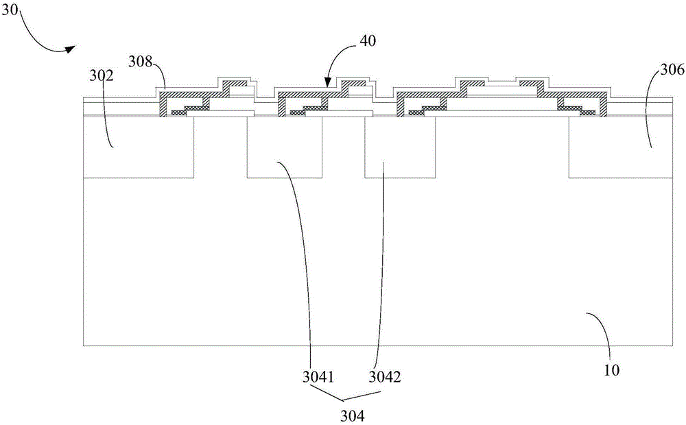
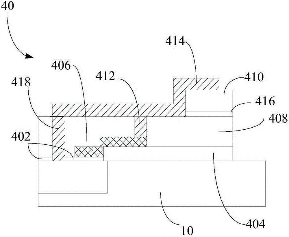
[0026] In order to make the object, technical solution and advantages of the present invention clearer, the present invention will be further described in detail below in conjunction with the accompanying drawings and embodiments. It should be understood that the specific embodiments described here are only used to explain the present invention, not to limit the present invention.

[0027] Unless otherwise defined, all technical and scientific terms used herein have the same meaning as commonly understood by one of ordinary skill in the technical field of the invention. The terms used herein in the description of the present invention are for the purpose of describing specific embodiments only, and are not intended to limit the present invention. As used herein, the term "and / or" includes any and all combinations of one or more of the associated listed items.

[0028] The vocabulary in the field of semiconductors cited in this article is a technical vocabulary commonly ...


PUM

PropertyMeasurementUnit
Thicknessaaaaaaaaaa
Thicknessaaaaaaaaaa

Abstract

The invention relates to a power transistor, which comprises a substrate, an active region and a terminal region, wherein the active region and the terminal region are formed on the substrate; the terminal region comprises a transition field limiting ring, field limiting rings, a cut-off ring and voltage-sharing protection structures; the transition field limiting ring, the field limiting rings and the cut-off ring are formed on the substrate and are sequentially arranged from inside to outside; gate oxidation layers in the voltage-sharing protection structures are formed on the surfaces of various doped regions; the field oxidation layers, first dielectric layers and second dielectric layers are formed on substrates at one side of various doped regions and are sequentially distributed upwards in a stepped form; the thickness of each field oxidation layer is greater than that of each gate oxidation layer; polysilicon field plates partially cover the gate oxidation layers and partially cover the field oxidation layers; first contact holes are formed in the first dielectric layers, run through the first dielectric layers and are connected to the polysilicon field plates; metal field plates partially cover the first dielectric layers and the second dielectric layers; and the metal field plates are connected with the polysilicon field plates through the first contact holes. The breakdown voltage of the power transistor is relatively high. The invention further relates to a manufacturing method of the power transistor.

Description

technical field [0001] The invention relates to the technical field of semiconductor preparation, in particular to a power transistor and a method for preparing the power transistor. Background technique [0002] High-voltage power transistors such as VDMOS (VerticalDouble-DiffusionMOSFET <metal-oxide-semiconductorfeld-effecttransistor>), the vertical double-diffused metal-oxide-semiconductor field-effect transistor) and the edge of the active region of the IGBT (InsulatedGateBipolarTransistor, insulated gate bipolar transistor) due to the electric field concentration effect of the cylindrical junction and spherical junction formed during ion implantation and diffusion, This reduces the breakdown voltage significantly. Traditional power transistors mostly use the combination of field limiting rings and polycrystalline field plates, and the combination of field limiting rings and metal field plates. Although these technologies can meet the conventional performance par...

Claims


Application Information

Patent Timeline
IPC IPC(8): H01L29/78H01L29/739H01L21/336H01L21/331H01L29/40
CPCH01L29/402H01L29/404H01L29/66325H01L29/66477H01L29/7393H01L29/78
Inventor 李学会
Owner 深圳深爱半导体股份有限公司
Why Eureka
Try Eureka