Two-dimensional wave beam scanning antenna array based on SIW (Substrate Integrated Waveguide)
A technology of beam scanning and antenna array, which is applied to antenna unit combinations with different polarization directions, resonant antennas, etc., can solve the problem of limited number of beam scanning, and achieve the effect of miniaturization design and size reduction
- Summary
- Abstract
- Description
- Claims
- Application Information
AI Technical Summary
Problems solved by technology
Method used
Image
Examples
Embodiment 1
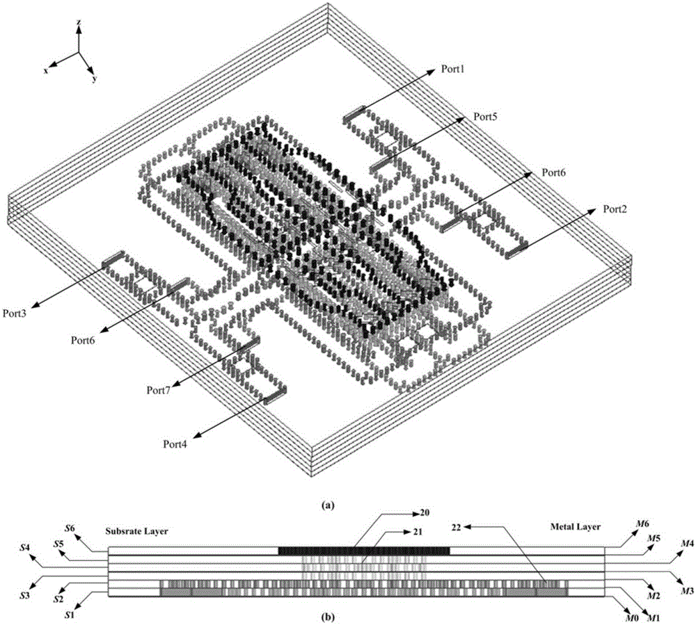
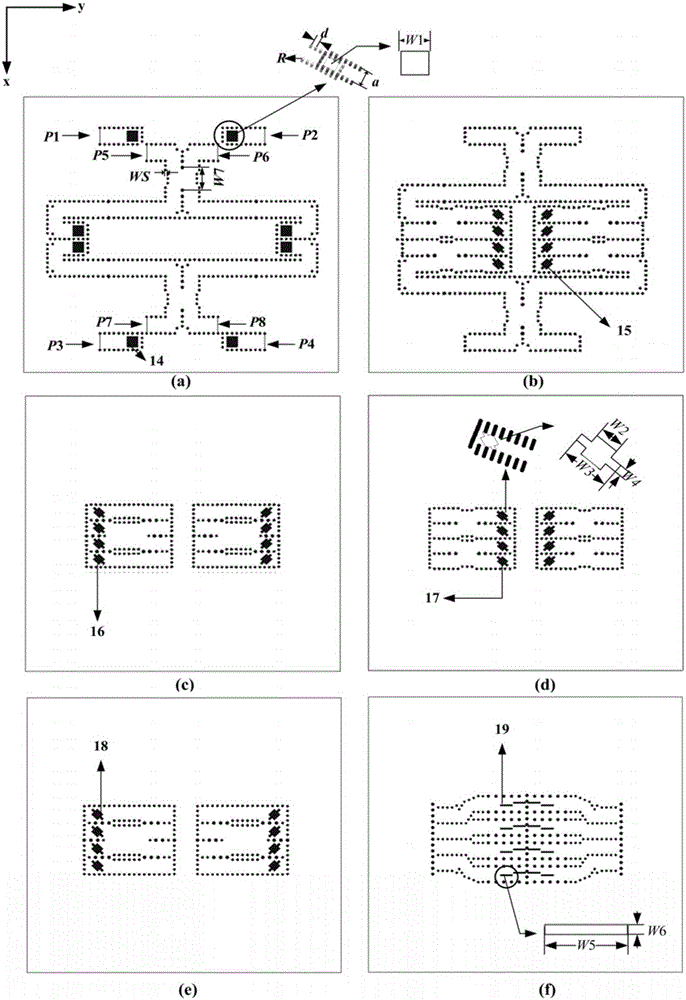
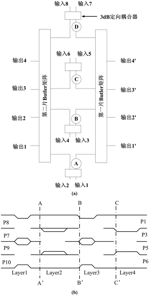
[0034] combine figure 1 , figure 2 with image 3 , the two-dimensional beam scanning array includes SIW slot antenna 20, dielectric substrate I [S1], dielectric substrate II [S2], dielectric substrate III [S3], dielectric substrate IV [S4], dielectric substrate V [S5], dielectric substrate Ⅵ[S6], metal layer [M0], metal layer Ⅰ[M1], metal layer Ⅱ[M2], metal layer Ⅲ[M3], metal layer Ⅳ[M4], metal layer Ⅴ[M5], metal layer Ⅵ[ M6], two Butler matrices 21 and a Butler matrix control network 22, the Butler matrix control network 22 controls the above two Butler matrices 21. The whole structure is composed of six dielectric substrates (18 layers of LTCC dielectric layers), where the dielectric constant of each dielectric substrate ε r is 5.9, the dielectric loss angle is 0.009, and the thickness H is 0.288mm, which is about 0.09λ 0 (where λ 0 is the free-space wavelength at 94GHz), and the width a of the SIW transmission structure of each layer of dielectric substrate is 1.086mm...
PUM
 Abstract
Description
Claims
Application Information


