Low power consumption boost circuit for electronic product

A technology for boosting circuits and electronic products, applied in electrical components, adjusting electrical variables, output power conversion devices, etc., can solve problems such as insufficient heat dissipation, noise, and interference in small-sized packages, and overcome EMI problems, electromagnetic interference, etc. The effect of low power consumption

Inactive Publication Date: 2015-12-23
成都米戈科技有限公司
View PDF0 Cites 1 Cited by
  • Summary
  • Abstract
  • Description
  • Claims
  • Application Information

AI Technical Summary

Problems solved by technology

[0002] The wide application of portable devices such as mobile phones has created a large number of new requirements for power management. In order to support increasingly complex system power requirements and new functions, major chip design companies have proposed advanced power supplies with different characteristics and smaller and smaller sizes. Management solutions, but the heat dissipation capability of small-size packages is not as good as that of large-size package products, forcing the conversion efficiency of devices to be improved, so switching regulators are replacing linear regulators to extend the working time, but the working time of portable devices such as mobile phones is still Can not meet people's needs, and the problems of noise and electromagnetic interference will follow

Method used


Image

  • Low power consumption boost circuit for electronic product

Examples


Embodiment Construction

[0011] The following will clearly and completely describe the technical solutions in the embodiments of the present invention with reference to the accompanying drawings in the embodiments of the present invention. Obviously, the described embodiments are only some, not all, embodiments of the present invention. Based on the embodiments of the present invention, all other embodiments obtained by persons of ordinary skill in the art without making creative efforts belong to the protection scope of the present invention.

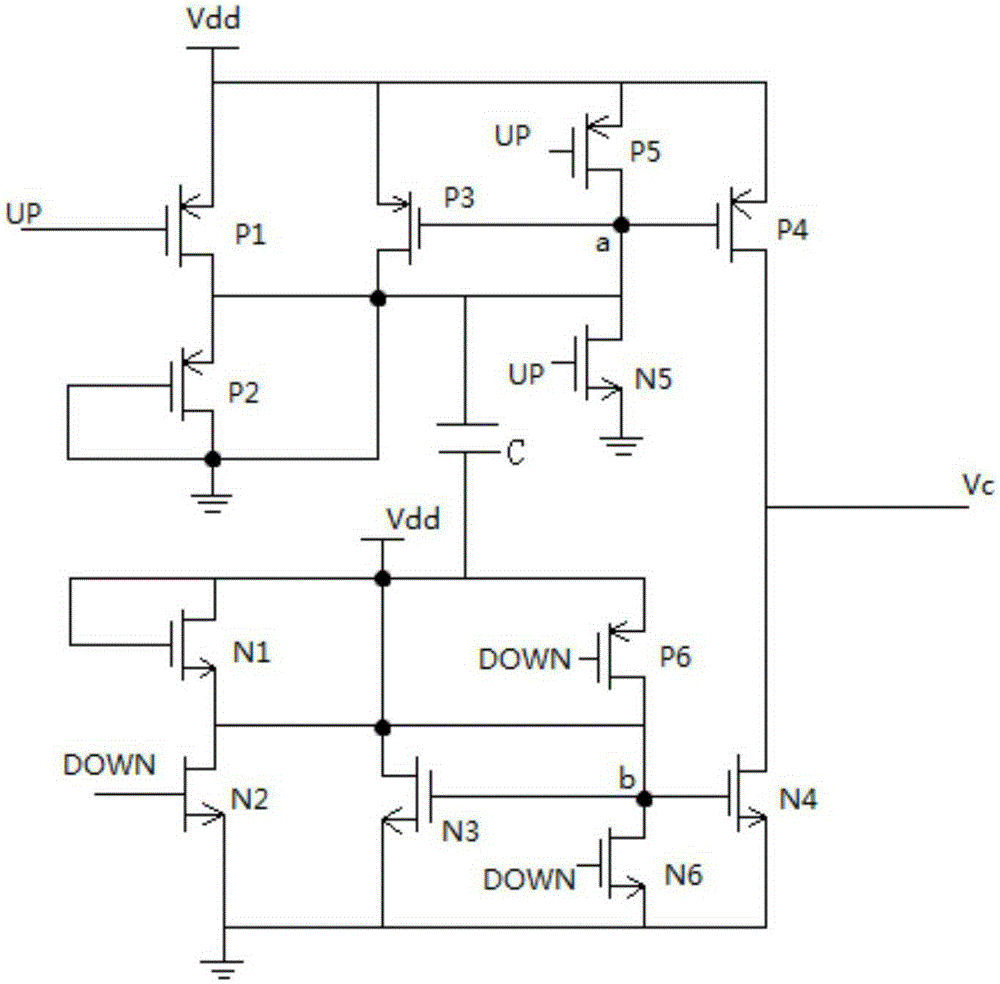
[0012] see figure 1 In an embodiment of the present invention, a low-power boost circuit for an electronic product includes a pull-up circuit and a pull-down circuit, the pull-up circuit includes a PMOS transistor P1 and a PMOS transistor P2, and the pull-down circuit includes an NMOS transistor N1 and an NMOS transistor N2 .

[0013] The G pole of the PMOS transistor P1 is connected to the UP signal input terminal, and the S pole of the PMOS transistor P1 is...


PUM


Abstract

The invention discloses a low power consumption boost circuit for an electronic product. The low power consumption boost circuit for an electronic product comprises a pull up circuit and a pull down circuit, wherein the pull up circuit comprises a PMOS pipe P1 and a PMOS pipe P2; the pull down circuit comprises an NMOS pipe N1 and an NMOS pipe N2; a G pole of the PMOS pipe P1 is connected with an UP signal input end; and the S pole of the PMOS pipe P1 is connected with a power supply Vdd, an S pole of a PMOS pipe P3, an S pole of a PMOS pipe P4 and an S pole of a PMOS pipe P5. Without requirement for external connection with inductance elements, the low power consumption boost circuit for an electronic product can realize boosting to a certain extent; as no inductance elements exist, the low power consumption boost circuit for an electronic product overcomes the EMI problem caused by the power source based on inductance; and the low power consumption boost circuit for an electronic product has the advantages of being low in generation of electromagnetic interference, being high in efficiency, being simple in circuit structure, being small in the occupied area, being low in power consumption, and being able to work with high efficiency when the power supply is under the low voltage condition.

Description

technical field [0001] The invention relates to a voltage boosting circuit, in particular to a low power consumption voltage boosting circuit for electronic products. Background technique [0002] The wide application of portable devices such as mobile phones has created a large number of new requirements for power management. In order to support increasingly complex system power requirements and new functions, major chip design companies have proposed advanced power supplies with different characteristics and smaller and smaller sizes. Management solutions, but the heat dissipation capability of small-size packages is not as good as that of large-size package products, forcing the conversion efficiency of devices to be improved, so switching regulators are replacing linear regulators to extend the working time, but the working time of portable devices such as mobile phones is still It cannot meet the needs of people, and the problems of noise and electromagnetic interferenc...

Claims


Application Information

Patent Timeline
Patent Type & Authority Applications(China)
IPC IPC(8): H02M3/155H02M3/07
Inventor 樊露
Owner 成都米戈科技有限公司
Why Eureka
Try Eureka