Integrating method for multiple metal gates
An integrated method and metal gate technology, applied in the manufacture of electrical components, circuits, semiconductors/solid-state devices, etc., can solve the problems of reducing device reliability, increasing thermal budget, poor alloy uniformity and controllability, etc., to reduce etching The number of times, improve the uniformity and controllability, reduce the effect of etching damage
- Summary
- Abstract
- Description
- Claims
- Application Information
AI Technical Summary
Problems solved by technology
Method used
Image

Examples
Embodiment 1
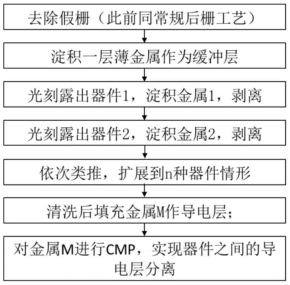
[0042] According to the following steps, three thresholds (Vt1, Vt2, Vt3 can be achieved; the specific values are based on the requirements of different technology generations and the performance of different types of devices (such as high-performance logic devices, low-power logic devices, I / O devices, etc.) Bulk silicon planar device for setup:
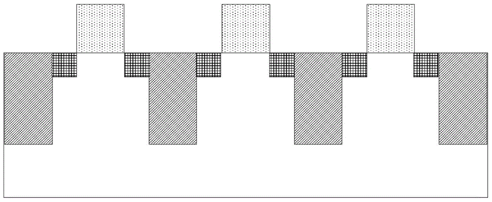
[0043] 1) Processed on a (100) bulk silicon substrate according to a standard bulk silicon plane process until the source / drain impurities are activated, such as figure 2 shown;
[0044] 2) PECVDSiO 2 as an isolation layer;
[0045] 3) CMPSiO 2 until the top of the false grid is exposed;
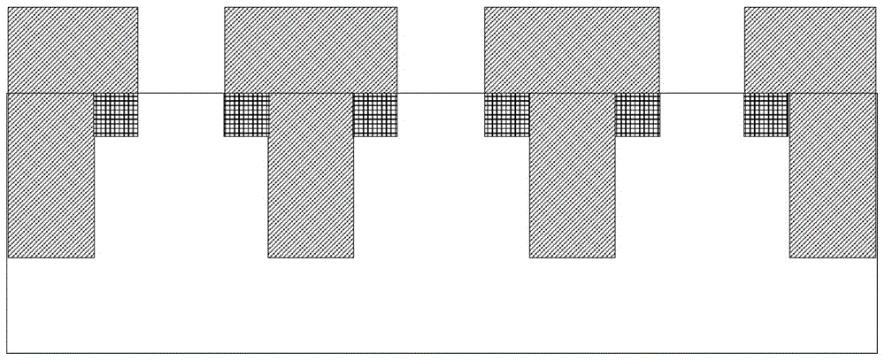
[0046] 4) Isotropic etching to remove false gates, such as image 3 shown;
[0047] 5) ALD1.5nmHfO2 is used as insulating gate dielectric;
[0048] 6) ALD5nmTaN as buffer layer, such as Figure 4 shown;
[0049] 7) The gate lines of the photolithographic device 1 (eg, having a threshold value Vt1) (the photoresist at the gate lines is ...
Embodiment 2
[0057] On the basis of Example 1, the following adjustments can be made to realize bulk silicon FinFET devices with three thresholds:
[0058] 1) In step 1 of Embodiment 1, the (100) bulk silicon substrate is processed according to the standard bulk silicon FinFET process until the source / drain impurities are activated;
[0059]2) In Step 5 of Embodiment 1, the type and thickness of the HK medium can be optimized and adjusted according to the actual technical node requirements;
[0060] 3) In steps 8 and 10 of embodiment 1, the type and thickness of metal 1, metal 2, and metal 3 can be optimized and adjusted according to the actual technical node requirements;
[0061] 4) In Step 11 of Embodiment 1, the type and thickness of the metal M can be optimized and adjusted according to the actual technical node requirements;
[0062] 5) In Step 13 of Embodiment 1, device integration is subsequently completed according to the standard bulk silicon FinFET back-end process.
PUM
 Abstract
Description
Claims
Application Information
 - R&D
- Intellectual Property
- Life Sciences
- Materials
- Tech Scout
- Unparalleled Data Quality
- Higher Quality Content
- 60% Fewer Hallucinations
Browse by: Latest US Patents, China's latest patents, Technical Efficacy Thesaurus, Application Domain, Technology Topic, Popular Technical Reports.
© 2025 PatSnap. All rights reserved.Legal|Privacy policy|Modern Slavery Act Transparency Statement|Sitemap|About US| Contact US: help@patsnap.com