Image sensor, and reading circuit and reading method of amorphous silicon TFT pixel unit

A technology of pixel unit and reading circuit, which is applied in the field of image sensors, can solve problems such as rising costs, achieve the effect of eliminating low-frequency noise and improving signal-to-noise ratio

Active Publication Date: 2015-12-30
SHANGHAI OXI TECH
View PDF4 Cites 7 Cited by
  • Summary
  • Abstract
  • Description
  • Claims
  • Application Information

AI Technical Summary

Problems solved by technology

When the photosensitive area of ​​a CMOS image sensor increases, its cost increases accordingly

Method used


Image

  • Image sensor, and reading circuit and reading method of amorphous silicon TFT pixel unit
  • Image sensor, and reading circuit and reading method of amorphous silicon TFT pixel unit
  • Image sensor, and reading circuit and reading method of amorphous silicon TFT pixel unit

Examples


Embodiment Construction

[0040] As described in the background art, due to the limitation of the amorphous silicon TFT process, the existing amorphous silicon photosensitive panel cannot integrate a complex pixel structure, and an external reading circuit is required to read the photocharge. The technical solution of the present invention provides an image sensor, a reading circuit and method for an amorphous silicon TFT pixel unit, the reading circuit of the amorphous silicon TFT pixel unit can generate a voltage signal proportional to the photocharge, and the voltage signal has High signal-to-noise ratio.

[0041] In order to make the above objects, features and advantages of the present invention more clearly understood, the specific embodiments of the present invention will be described in detail below with reference to the accompanying drawings.

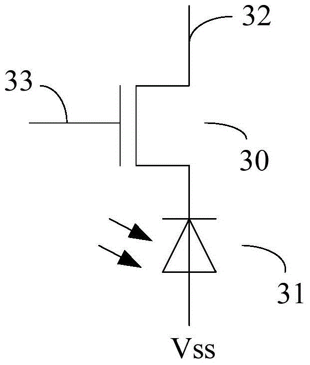
[0042] Figure 4 It is a schematic structural diagram of a reading circuit of an amorphous silicon TFT pixel unit according to an embodiment of the pr...


PUM


Abstract

An image sensor, and a reading circuit and a reading method of an amorphous silicon TFT pixel unit are provided. The amorphous silicon TFT pixel unit comprises an amorphous silicon TFT and a photoelectric diode. The reading circuit of the amorphous silicon TFT pixel unit comprises an operational amplifier, a first capacitor, a first switch, a second switch, a third switch, and a sampling and holding unit. According to the image sensor, and the reading circuit and the reading method of the amorphous silicon TFT pixel unit provided by the invention, the signal-to-noise ratio of the output signal of the reading circuit of the amorphous silicon TFT pixel unit is improved.

Description

technical field [0001] The present invention relates to the technical field of image sensors, in particular to an image sensor, a reading circuit and a method for an amorphous silicon TFT pixel unit. Background technique [0002] As a very old biometric identification method, fingerprint identification has recently attracted widespread attention, especially its application in mobile payment has brought broad development prospects. As a key device for automatic fingerprint collection, fingerprint image sensor is mainly divided into two categories: optical fingerprint image sensor and semiconductor fingerprint image sensor. [0003] figure 1 It is a schematic diagram of the light-sensing circuit using an optical fingerprint image sensor to collect fingerprints. During fingerprint collection, the finger 11 is attached to the optical lens 12 , and the light emitted by the light source 13 is refracted on the finger 11 through the first prism 14 . The finger 11 is irradiated by...

Claims


Application Information

Patent Timeline
Patent Type & Authority Applications(China)
IPC IPC(8): H04N5/335H04N5/341H04N5/378
Inventor 林崴平
Owner SHANGHAI OXI TECH
Why Eureka
Try Eureka