
Semiconductor plasma processing device capable of improving appearance of film at surface of wafer

A processing device and semiconductor technology, applied in discharge tubes, electrical components, circuits, etc., can solve the problems of uneven plasma distribution, electric field bending, uneven edge film, etc., to avoid excessive growth, uniform growth, and reduce gas flow. Effect

Active Publication Date: 2016-01-06
PIOTECH CO LTD
View PDF10 Cites 6 Cited by
  • Summary
  • Abstract
  • Description
  • Claims
  • Application Information

AI Technical Summary

Problems solved by technology

Under the action of the shower head and the gas pumping ceramic ring in the prior art, since the gas is distributed outward from the center of the stage, it is easy to cause uneven distribution of peripheral gas, resulting in uneven distribution of plasma; in addition, the plasma is affected by The electric field control is affected by the upper and lower plates near the edge of the two plates, which causes the electric field to bend, which in turn leads to uneven distribution of the plasma, and in both cases, affects the deposition rate of the film on the wafer surface, resulting in edge film uneven
[0004] With the rapid development of semiconductor technology, the area of ​​wafers to be processed will continue to increase. In the prior art, the problem of uneven accumulation of wafer films caused by shower heads with evenly distributed through holes and ceramic rings with fixed air extraction holes will become more serious. Prominent, in summary, it is necessary to improve the hardware in the semiconductor plasma processing device, improve the uniformity of the plasma distribution of the process gas, and improve the surface morphology of the film on the wafer surface

Method used


Image

  • Semiconductor plasma processing device capable of improving appearance of film at surface of wafer
  • Semiconductor plasma processing device capable of improving appearance of film at surface of wafer
  • Semiconductor plasma processing device capable of improving appearance of film at surface of wafer

Examples


Embodiment 1

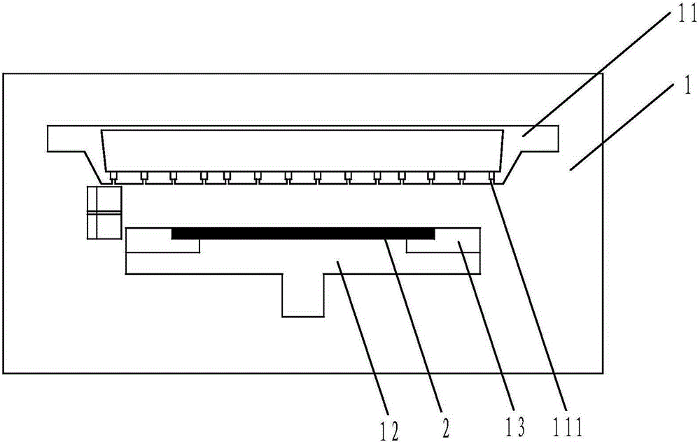
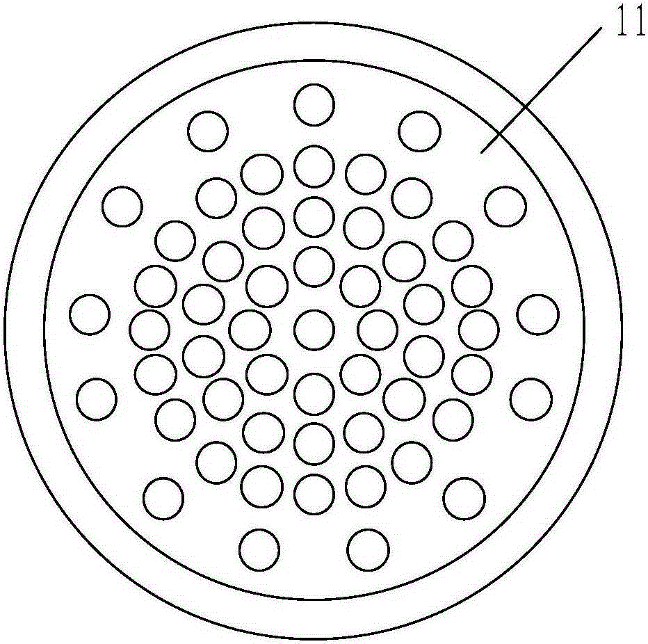
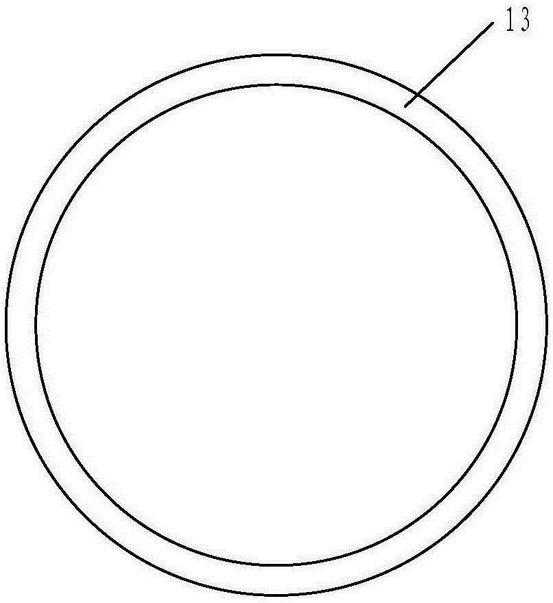
[0028] The process experiment was carried out using a semiconductor plasma processing device with 1 to 5 rings of through holes 111 reduced by 10% on the periphery of the shower head 11 and the air extraction hole 131 of the air extraction ceramic ring 13 moved down by 3 mm. The substrate used in the experiment was a 300 mm silicon wafer. During the experiment, the process gas was supplied to the stage 12 from the through hole 111 of the shower head 11, and the gas was exhausted from the exhaust hole 131 of the pumping ceramic ring 13 around the stage 12, and the pressure was stabilized by the control device. Afterwards, the shower head 11 and the stage 12 are used as the upper and lower electrodes to apply a voltage to form a plasma field between the shower head 11 and the stage 12 to perform plasma treatment on the loaded objects.

Embodiment 2

[0030] A semiconductor plasma processing device with 1 to 5 circles of through holes 111 reduced by 35% on the periphery of the shower head 11 and the air extraction hole 131 of the air extraction ceramic ring 13 moved down by 8 mm was used for the process experiment. The substrate used in the experiment was a 300 mm silicon wafer. During the experiment, the process gas was supplied to the stage 12 from the through hole 111 of the shower head 11, and the gas was exhausted from the exhaust hole 131 of the pumping ceramic ring 13 around the stage 12, and the pressure was stabilized by the control device. Afterwards, the shower head 11 and the stage 12 are used as the upper and lower electrodes to apply a voltage to form a plasma field between the shower head 11 and the stage 12 to perform plasma treatment on the loaded objects.

Embodiment 3

[0032] A process experiment was carried out using a semiconductor plasma processing device with 1 to 5 rings of through holes 111 reduced by 60% on the periphery of the shower head 11 and the air extraction holes 131 of the air extraction ceramic ring 13 moved down by 15 mm. The substrate used in the experiment was a 300 mm silicon wafer. During the experiment, the process gas was supplied to the stage 12 from the through hole 111 of the shower head 11, and the gas was exhausted from the exhaust hole 131 of the pumping ceramic ring 13 around the stage 12, and the pressure was stabilized by the control device. Afterwards, the shower head 11 and the stage 12 are used as the upper and lower electrodes to apply a voltage to form a plasma field between the shower head 11 and the stage 12 to perform plasma treatment on the loaded objects.

[0033] Figure 6 The results of Examples 1, 2, and 3 are counted, and the center of circle of the silicon wafer is obtained as the origin, the x...


PUM


Abstract

The invention provides a semiconductor plasma processing device capable of improving the appearance of a film at the surface of a wafer. The processing device comprises a reaction cavity and the wafer to be processed, the reaction cavity is internally provided with a spray head, an objective table and an exhausting ceramic ring, edge holes are distributed non-uniformly in the spray head, an exhausting hole of the exhausting ceramic ring moves downwardly, and the spray head is placed opposite to the objective table in the reaction cavity. The amount of edge holes of the spray head is reduced to reduce gas flow at the edge of the wafer, and the film at the edge of the wafer is avoided from too fast growth; the position of the exhausting hole of the exhausting ceramic ring moves downwardly to change the air flow path of exhausting and adjust the deposition effect of the substrate surface; and the film can grow uniformly on the substrate due to novel design of the spray head and exhausting ceramic ring in the device.

Description

technical field [0001] The invention belongs to the technical field of semiconductor manufacturing and application, and in particular relates to a semiconductor plasma processing device for improving the morphology of a thin film on the surface of a wafer. By using the device, the thin film on the edge of the wafer can be grown uniformly. Background technique [0002] The semiconductor plasma processing device in the prior art generally has a shower head as the upper plate and a stage as the lower plate in the reaction chamber, and by applying a stable voltage between the two, the spray head The gas ejected from the head is plasmaized, and the wafer is plasma treated. The shower head used has through holes for the gas to be ejected. The through holes are evenly distributed in the center and edge of the shower head. [0003] The stage is used as the base to carry the wafer, and a pumping ceramic ring is fixed around the stage, and the pumping holes are uniformly and centrally...

Claims


Application Information

Patent Timeline
Patent Type & Authority Applications(China)
IPC IPC(8): H01J37/32
Inventor 戚艳丽杨艳宁建平
Owner PIOTECH CO LTD
Learn More