Large-sized light-emitting diode

A light-emitting diode, large-scale technology, applied in electrical components, circuits, semiconductor devices, etc., can solve the problems of low luminous efficiency of diodes, poor current expansion effect of single-layer ITO conductive layer, and large light-blocking area of ​​extended electrodes, and achieves high efficiency. Current spreading effect, increasing current spreading effect, improving luminous efficiency

Inactive Publication Date: 2016-01-06
XIAMEN CHANGELIGHT CO LTD
View PDF4 Cites 1 Cited by
  • Summary
  • Abstract
  • Description
  • Claims
  • Application Information

AI Technical Summary

Problems solved by technology

[0004] The current spreading effect of the single-layer ITO conductive layer is poor, which makes the light-shielding area of ​​the extended electrode larger, which in turn makes the diode luminous efficiency lower

Method used


Image

  • Large-sized light-emitting diode
  • Large-sized light-emitting diode
  • Large-sized light-emitting diode

Examples


Embodiment Construction

[0066] The present invention will be described in detail below in conjunction with the accompanying drawings and specific embodiments.

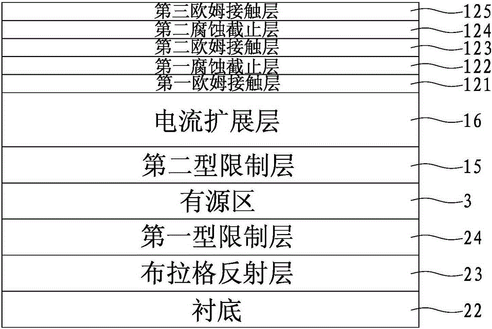
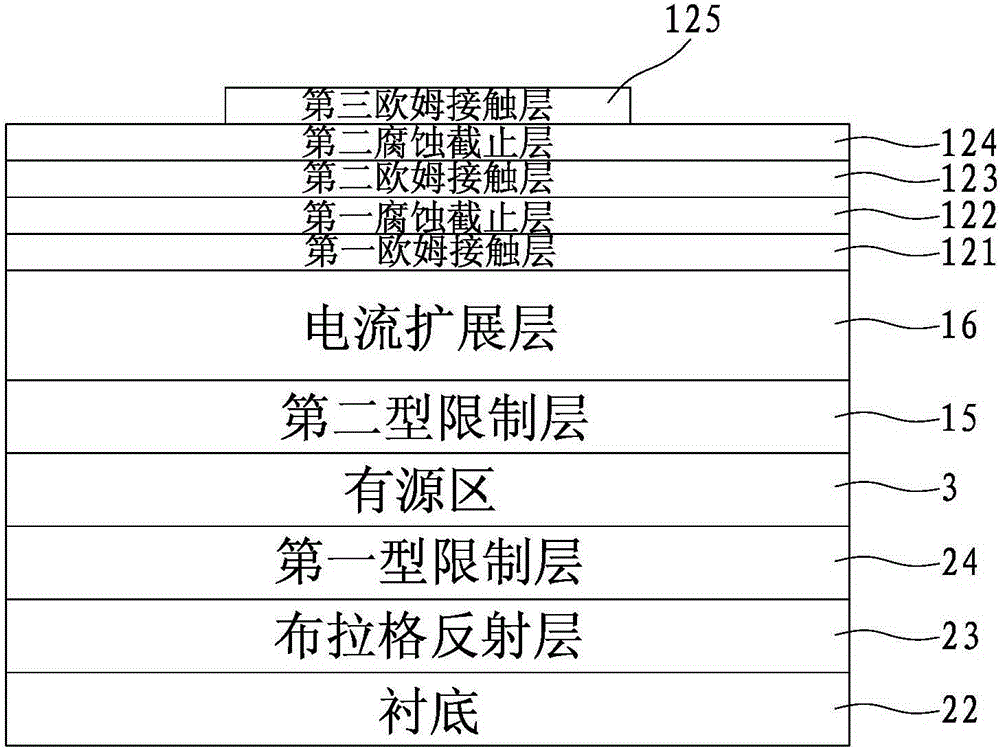
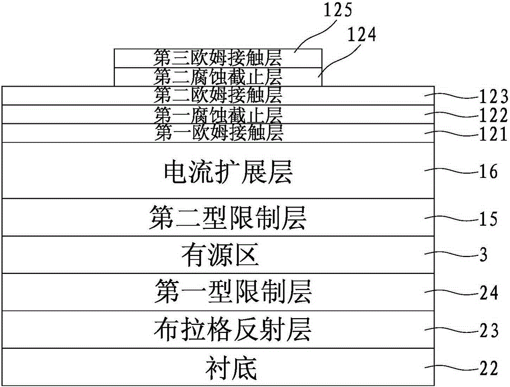
[0067] refer to Figure 1 to Figure 6a As shown, the first embodiment of a large-size light-emitting diode disclosed by the present invention, such as Figure 6a As shown, it includes a p region 1, an n region 2 and an active region 3. The active region 3 is arranged between the p region 1 and the n region 2, the first electrode 11 is arranged on the p region 1, and the first electrode 11 is arranged on the n region 2. the second electrode 21 .

[0068] The p region 1 is provided with a composite multilayer ohmic contact layer structure 12 , an ITO conductive layer 13 is evaporated on the composite multilayer ohmic contact layer structure 12 , and the first electrode 11 is provided on the ITO conductive layer 13 . In this embodiment, the structure of the composite multilayer ohmic contact layer 12 is that corrosion stop layers are respectiv...


PUM


Abstract

The invention discloses a large-sized light-emitting diode. The large-sized light-emitting diode includes a p region, an n region and an active region, wherein the active region is arranged between the p region and the n region, the p region is provided with a first electrode, and the n region is provided with a second electrode. The large-sized light-emitting diode is characterized in that the p region is provided with a composite multilayer ohmic contact layer structure; an ITO electric conduction layer is formed on the composite multilayer ohmic contact layer structure through evaporation; and the first electrode is arranged on the ITO electric conduction layer. According to the large-sized light-emitting diode of the invention, the current expansion effect of the ITO electric conduction layer can be improved, and the light shielding area of the expansion electrodes can be reduced, and therefore, the luminous efficiency of the light-emitting diode can be improved, and manufacturing cost can be reduced.

Description

technical field [0001] The invention relates to the technical field of light-emitting diodes, in particular to a large-size light-emitting diode. Background technique [0002] In the prior art, a large-sized light-emitting diode includes a p region, an n region and an active region, the active region is arranged between the p region and the n region, and the first electrode is arranged on the ITO (indium tin oxide) conductive layer of the p region (p-electrode); a second electrode (n-electrode) is provided on the substrate of the n-region. [0003] The large-size light-emitting diodes usually have a confinement layer on the active region, a current spreading layer on the confinement layer, an ohmic contact layer on the current spreading layer, and ITO is directly deposited on the single-layer ohmic contact layer ( indium tin oxide) conductive layer, its defects are: [0004] The current spreading effect of the single-layer ITO conductive layer is poor, so that the light-sh...

Claims


Application Information

Patent Timeline
IPC IPC(8): H01L33/38H01L33/42
CPCH01L33/38H01L33/42H01L2933/0016
Inventor 林志伟陈凯轩张永姜伟卓祥景方天足陈亮
Owner XIAMEN CHANGELIGHT CO LTD
Why Eureka
Try Eureka