Photoresist coating device and lithography equipment

A technology of coating device and exposure device, which is applied in the direction of microlithography exposure equipment, photoplate-making process coating equipment, photoplate-making process exposure device, etc., can solve the problems of exhaust pipe leakage, temperature drop, equipment abnormality, etc. Achieve the effects of protecting the environment, reducing production costs, and improving operating efficiency

Inactive Publication Date: 2016-01-13
WUHAN CHINA STAR OPTOELECTRONICS TECH CO LTD
View PDF2 Cites 12 Cited by
  • Summary
  • Abstract
  • Description
  • Claims
  • Application Information

AI Technical Summary

Problems solved by technology

However, the temperature of the gaseous PGMEA solvent in the exhaust pipe will decrease, the pressure will increase, and the vapor of the PGMEA solvent will be liquefied. Abnormal or leakage of exhaust pipe occurs
In addition, the gaseous PGMEA solvent is treated as waste gas, causing pollution to the environment

Method used


Image

  • Photoresist coating device and lithography equipment
  • Photoresist coating device and lithography equipment

Examples


Embodiment Construction

[0019] In order to make the objectives, technical solutions, and advantages of the present invention clearer, the specific embodiments of the present invention will be described in detail below with reference to the accompanying drawings. Examples of these preferred embodiments are illustrated in the drawings. The embodiments of the present invention shown in the drawings and described in accordance with the drawings are merely exemplary, and the present invention is not limited to these embodiments.

[0020] Here, it should also be noted that, in order to avoid obscuring the present invention due to unnecessary details, only the structure and / or processing steps closely related to the solution according to the present invention are shown in the drawings, and the Other details not relevant to the present invention.

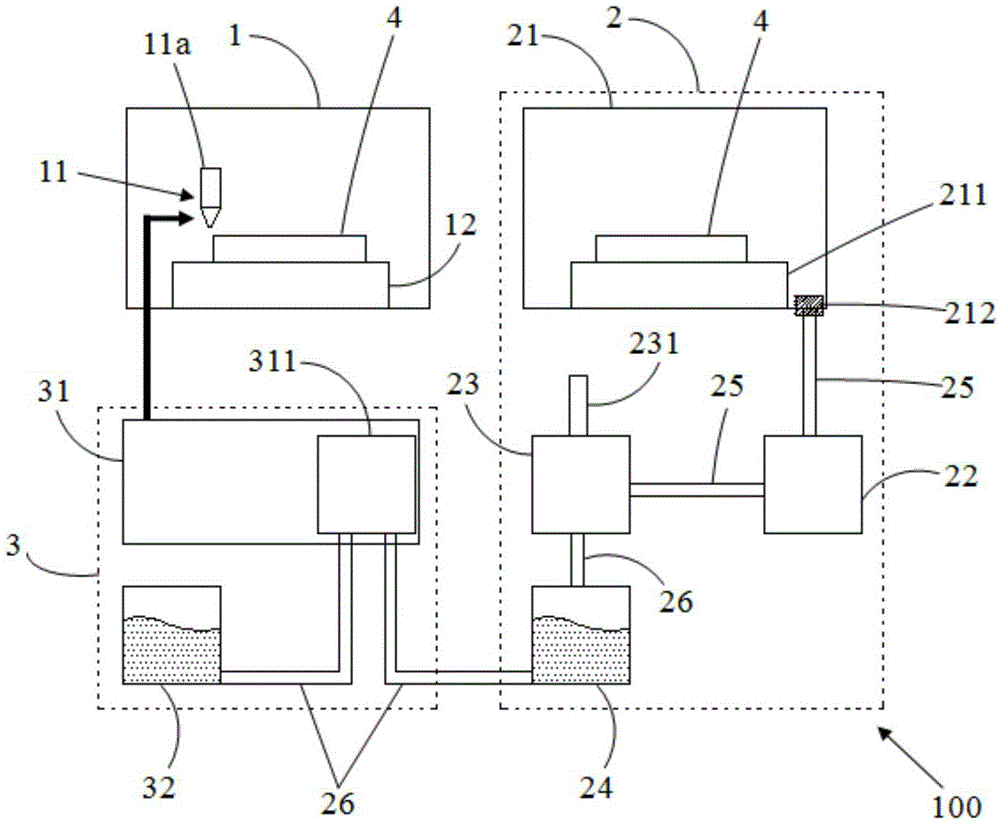
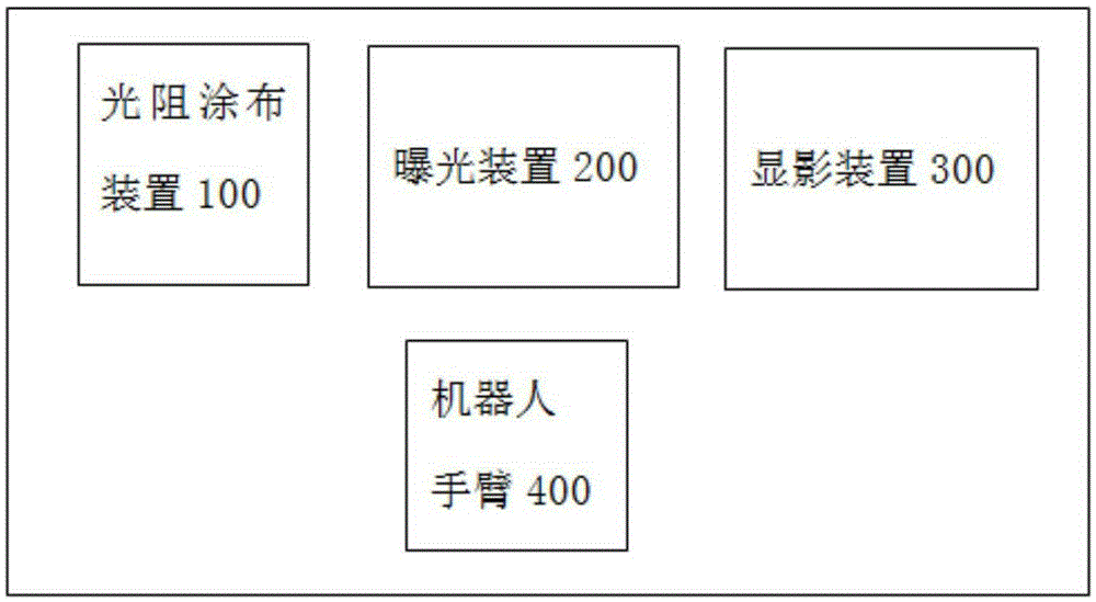
[0021] This embodiment first provides a photoresist coating device, such as figure 1 As shown, the photoresist coating device 100 includes a coating unit 1, a drying ...


PUM


Abstract

The invention discloses a photoresist coating device, comprising a coating unit, a drying unit and a cleaning unit. The coating unit comprises a spraying mechanism; the spraying mechanism is for spraying a photoresist material on a glass substrate; the drying unit comprises a drying chamber for evaporation and vaporization of a solvent in the photoresist material on the glass substrate; a vacuum pump is connected with the drying chamber and for discharging the vaporized solvent; a condenser is connected with the vacuum pump, and is used for condensing the liquefying gaseous solvent; a recycling container is connected with the condenser, and is for the storage of the liquefied solvent; the cleaning unit is connected between the recycling container and the coating unit; and solvent is obtained from the recycling container, and the solvent is used for cleaning the spraying mechanism. The invention also discloses lithography equipment containing the above photoresist coating device.

Description

Technical field [0001] The present invention relates to the technical field of display manufacturing, in particular to a photoresist coating device, and also relates to a photolithography equipment containing the photoresist coating device. Background technique [0002] The thin film transistor array substrate (TFT-Array) is one of the important components in the thin film transistor liquid crystal display (TFT-LCD). The production of the thin film transistor array substrate usually includes multiple masking processes (patterning processes), and each mask process It includes the steps of photoresist coating, exposure, development, etching and photoresist stripping on the glass substrate. [0003] Among them, in the photoresist coating step, the photoresist material needs to be sprayed on the glass substrate through a nozzle. In order to be easily coated on the glass substrate, a large amount of solvent (solvent) is added to the photoresist material, which is usually Propylene glyc...

Claims


Application Information

Patent Timeline
Patent Type & Authority Applications(China)
IPC IPC(8): G03F7/16G03F7/20
Inventor 欧阳志华
Owner WUHAN CHINA STAR OPTOELECTRONICS TECH CO LTD
Why Eureka
Try Eureka