
Method for forming self-aligned split-gate flash memory

A separate gate and self-alignment technology, which is applied in semiconductor devices, electrical components, circuits, etc., can solve the problems of unfavorable low and medium density, increase decoding devices, weaken the effect of cost reduction, etc., to ensure reading speed and programming efficiency Effect

Active Publication Date: 2021-01-29
董业民
View PDF6 Cites 0 Cited by
  • Summary
  • Abstract
  • Description
  • Claims
  • Application Information

AI Technical Summary

Problems solved by technology

[0005] Like the mainstream logic CMOS process, continuous reduction of cell area and cost reduction are also the main direction of flash memory development. From the published data, with the reduction of cell area, it is often necessary to add additional ports, such as control gates, erase Gate, etc., which brings additional complexity to the design, requires additional decoding devices, and increases the area of ​​the peripheral area, which is especially unfavorable for the application of low-to-medium density, and weakens the cost reduction effect brought about by the reduction of unit size.

Method used


Image

  • Method for forming self-aligned split-gate flash memory
  • Method for forming self-aligned split-gate flash memory
  • Method for forming self-aligned split-gate flash memory

Examples


Embodiment Construction

[0018] In order to make the above objects, features and advantages of the present invention more comprehensible, specific embodiments of the present invention will be described in detail below in conjunction with the accompanying drawings.

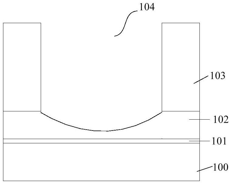
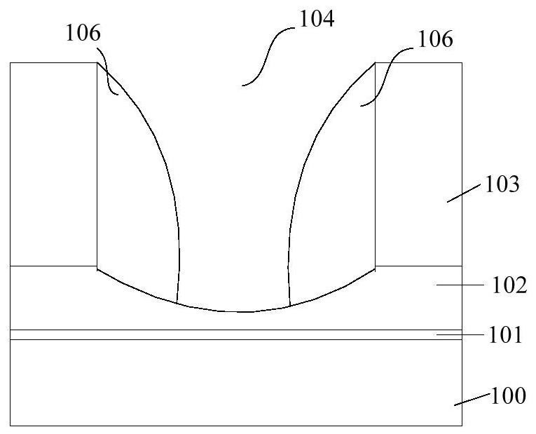
[0019] Figure 1 to Figure 6 A schematic cross-sectional view of a flash memory cell with a self-aligned split gate structure according to an embodiment is schematically given.

[0020] Please refer to figure 1 A substrate 100 is provided, and a thermal oxide layer 101 , a floating gate layer 102 and a hard mask layer 103 are sequentially grown on the surface of the substrate 100 .

[0021] The material of the substrate 100 is semiconductor silicon, which can be n-type or p-type semiconductor, or silicon-on-insulator etc. bottom), graded substrates, silicon-on-insulator substrates, epitaxial silicon substrates, partially processed substrates (including parts of integrated circuits and other components), patterned or unpatterned substrate...


PUM

PropertyMeasurementUnit
thicknessaaaaaaaaaa
thicknessaaaaaaaaaa
thicknessaaaaaaaaaa

Abstract

A method for forming a self-aligned split-gate flash memory, comprising: sequentially forming a thermal oxide layer, a floating gate layer, and a hard mask layer on the surface of a substrate, the hard mask layer having an opening exposing the thermal oxide layer; An ONO layer is formed on the surface of the mask layer and in the opening; a composite layer is formed on the surface of the ONO layer; the composite layer and the ONO layer are etched by an etching process until the surface of the hard mask layer and the surface of the floating gate layer are exposed , forming sidewalls on both sides of the first opening, and the sidewalls are located on the surface of the ONO layer at the bottom of the first opening; using the sidewalls as a mask to etch the floating gate layer and the thermal oxide layer; The first spacer on the top surface of the wall and the second sidewall on the side of the sidewall, the floating gate layer and the thermal oxide layer; fill the first opening with the polysilicon layer, and planarize the polysilicon layer until the exposed On the surface of the hard mask layer, a structure in which the control gate and the source line are integrated is formed. Embodiments of the present invention do not need additional ports.

Description

technical field [0001] The invention relates to the field of semiconductor manufacturing, in particular to a method for forming a self-aligned split-gate flash memory. Background technique [0002] Flash memory is an important non-volatile semiconductor memory. Flash memory has the advantages of high storage density, low cost, and good reliability, and is widely used in industrial control, mobile phones, and communications. The basic principle of flash memory is to change the switching state of memory cells by injecting and erasing charges (electrons) on the floating gate of flash memory, so as to achieve the purpose of storing data. [0003] From the basic classification of architecture, flash memory is divided into two types: NAND and NOR. NAND is more suitable for mass data storage, requiring high-density storage units and low cost; NOR is more suitable for program storage, requiring random readability, high-speed reading, and directly exchanging information with microp...

Claims


Application Information

Patent Timeline
Patent Type & Authority Patents(China)
IPC IPC(8): H01L27/11521H01L21/28H10B41/30
CPCH01L21/28H10B41/00
Inventor 董业民
Owner 董业民
Features
  • Generate Ideas
  • Intellectual Property
  • Life Sciences
  • Materials
  • Tech Scout
  • Unparalleled Data Quality
  • Higher Quality Content
  • 60% Fewer Hallucinations
Learn More